


Leveraging decades of expertise, Samco offers high precision and high-speed etching of Silicon and related materials.
Samco was the first of Japan’s semiconductor process equipment manufacturers to obtain a Bosch Process license. Using our latest patented Tornado ICP® technology and harnessing the Bosch Process, Samco’s Si DRIE systems have proven effective in deep, vertical, high-speed Si deep etching for both R&D and production. Also, Samco developed high precision processing at the nano level using ICP etching and RIE systems.
Samco offers Deep Reactive Ion Etching (DRIE or Deep RIE) of Silicon, using the Bosch process for MEMS and TSV applications.
The Bosch Process is a high-aspect ratio etching technology, which repeats the cycle of isotropic etching followed by protection film deposition. The SF6 plasma cycle etches silicon, and the C4F8 plasma cycle creates a protection layer. Combining this process technique with our latest system technology has produced industry leading results for both research and manufacturing customers.
The Bosch Process is a high-aspect ratio etching technology, which repeats the cycle of isotropic etching followed by protection film deposition. The SF6 plasma cycle etches silicon, and the C4F8 plasma cycle creates a protection layer. Combining this process technique with our latest system technology has produced industry leading results for both research and manufacturing customers.
Samco was the first Japanese semiconductor process equipment manufacturer to offer Deep Reactive Ion Etching (DRIE or Deep RIE) systems using the Bosch Process for MEMS and TSV fabrication.
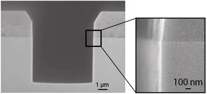
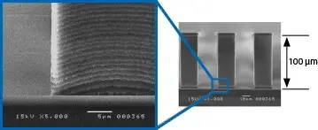
Scallops are formed during the switch from etch to deposition cycles of the silicon Bosch Process. Slow-speed gas switching can result in large scallops and rough sidewalls, and they deteriorate device performance. Samco has developed a smooth sidewall process using 0.1 second high-speed gas switching so that the scallop size is controlled to less than 5 nm while still retaining an etch rate of 2 μm/min. This process is applicable to Cu metallization of Through Silicon Via (TSV) and nanoimprint mold fabrication.
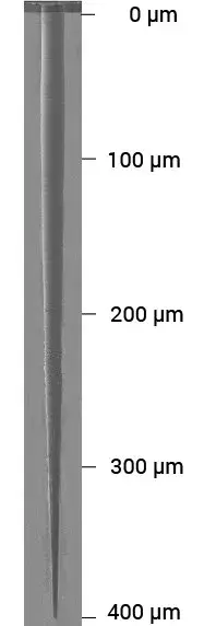
400
µm Deep
27
Aspect Ratio
47
Selectivity (Si/PR)
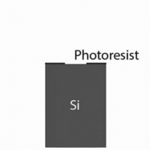
One of the challenges in deep silicon etching is reliable profile control. Bowing and side-etch caused by protection film break are typical failure in Si deep hole etching.
This 400 µm deep tapered profile (ø 15 µm) was fabricated with process optimization. The profile shows aspect ratio of 27, and tilt is controlled within 90 ° +/- 0.3 °.
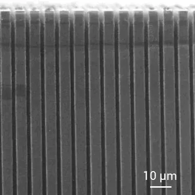
55
µm/min
An etch rate of 55 µm/min is achieved using an efficient ICP RF power source and improved pumping dynamics. The pattern width is 50 µm.
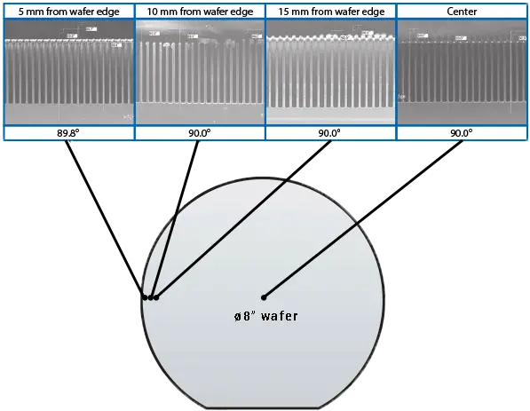
90°
Vertical Profile
In the Bosch process, at the edge of a wafer, the etch profile can become “tilted”. Precise tilt control is critical in some applications such as TSV fabrication. A tilt angle of just 1° could result in the misalignment of a 200 μm thick TSV by as much as 2 μm. Samco has developed tilt-free processes for both ø6″ and 8”wafers.
40
Aspect Ratio
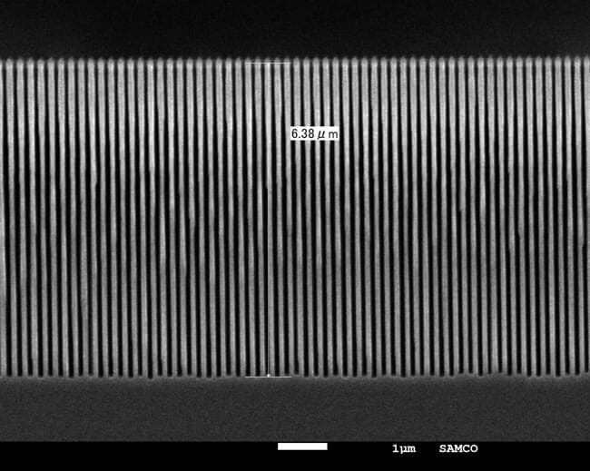
High-aspect-ratio silicon deep etching with a pattern width of 80 nm and a depth of 6380 nm was achieved using the Bosch process.
Comb-shape arrays with nanoscale-gap were fabricated for a MEMS capacitive accelerometer.
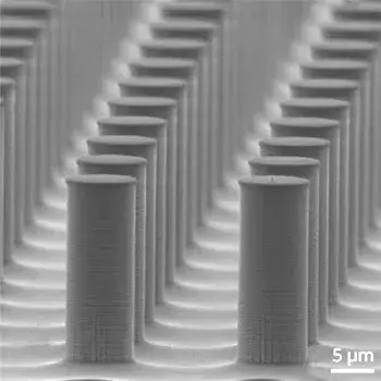
30 µm deep pillars with different sizes and densities were fabricated.
The pillar distribution worked for fast analysis time under high flow rate condition.
A 15 µm thick silicon layer on a silicon-on-glass (SOG) substrate was etched using notch-free SOI etching process that maintains the etch selectivity by using superimposed Radio Frequency (RF) power.
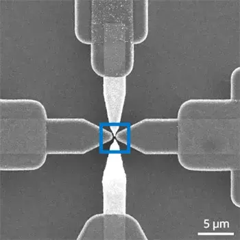
MEMS structures fabricated using the Bosch Process to integrate field-effect transistor (FET) with single-walled carbon nanotubes. Terminals were separated with sub-micron gaps by the anisotropic etch process.
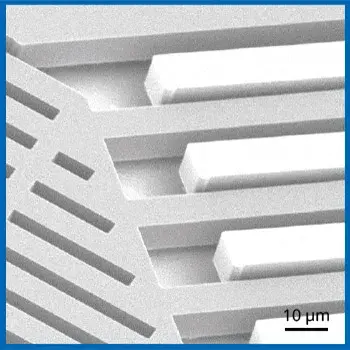
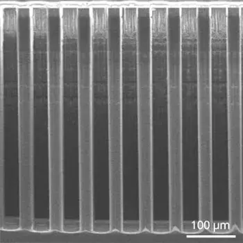
2 mm wide large-area etching with smooth sidewalls and flat bottom without any grasses and pits.
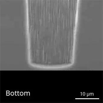
Deep holes with control profile from vertical to tapered can be fabricated without undercut. The profile has smooth sidewalls , improving TSV performance and reliability by reducing resistance and signal loss.
Pillar fabrication is an application of silicon DRIE, suitable for various devices such as microfluidics and optical MEMS. Using the Bosch process, silicon pillars with a diameter of Ø10 µm and a height of 20 µm were fabricated, featuring sidewall scallop widths of less than 100 nm.
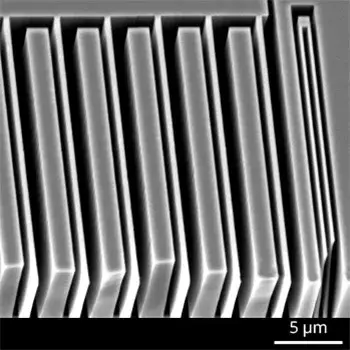
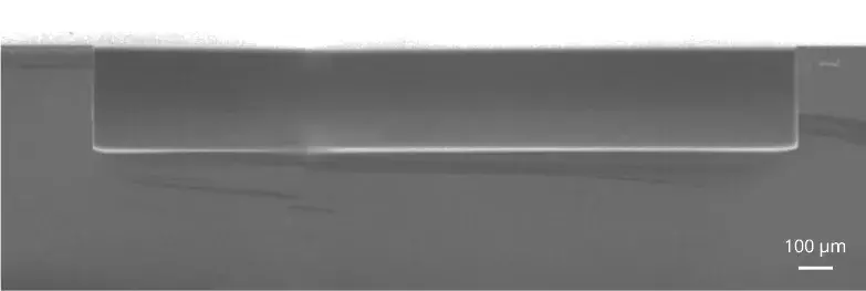
Square-shaped pillars with a width of 28 μm and a height of 450 μm were fabricated using the Bosch process. The pillars maintained a consistent square profile from top to bottom, with a precise profile angle of 89.9°.
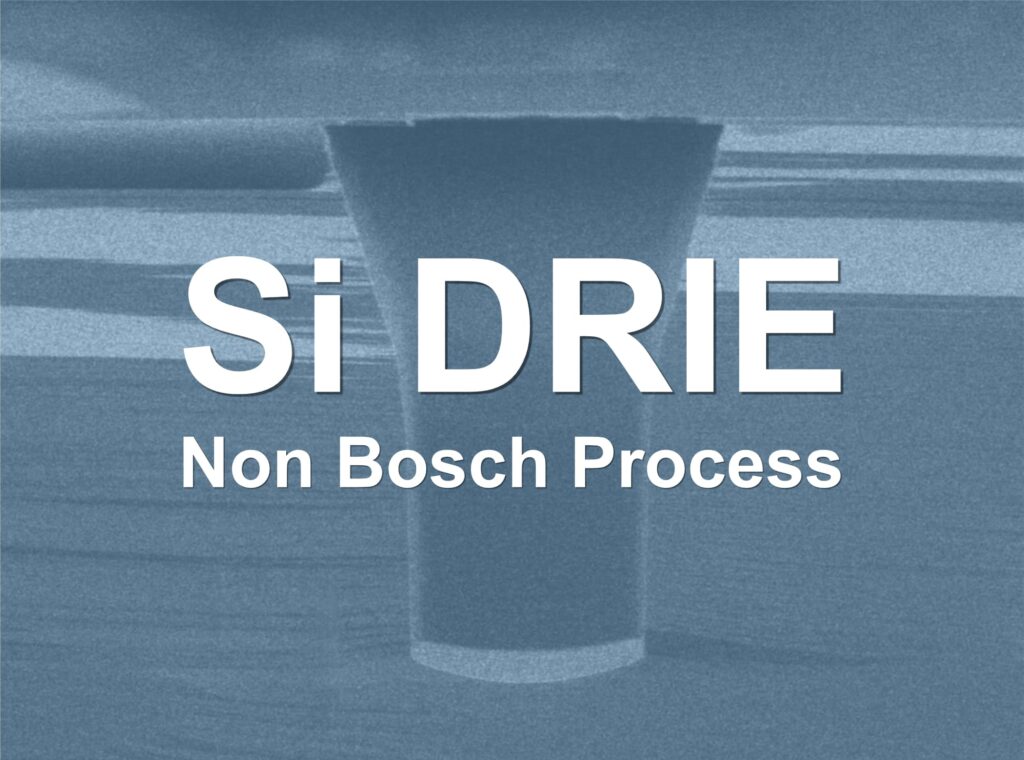
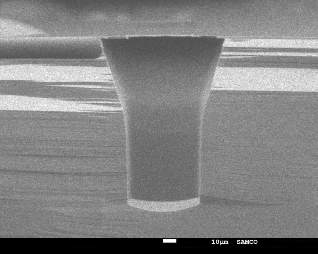
Samco provides high-rate Si Deep Reactive Ion Etching (DRIE) using a non-Bosch process, offering a solution to eliminate sidewall scallops typically associated with Bosch-based etching. This innovative approach ensures smooth sidewalls, even for etch depths exceeding 100 μm, making it an ideal choice for demanding applications such as Through Silicon Via (TSV) formation in 3D LSI electrode structures.
The non-Bosch DRIE process achieves precise etching profiles while maintaining high throughput, delivering superior results for advanced semiconductor and MEMS device fabrication.
High-rate Si DRIE with a depth of 126 μm for a 50 μm hole pattern using a non-Bosch process. The upper part of the etched profile is adjusted to a forward taper of 73° with no bowing.
Nano-level Si DRIE with line & space = 150/50 nm is achieved by the non-Bosch process. Samco’s unique solution provides precise Si DRIE with an aspect ratio of 5:1.