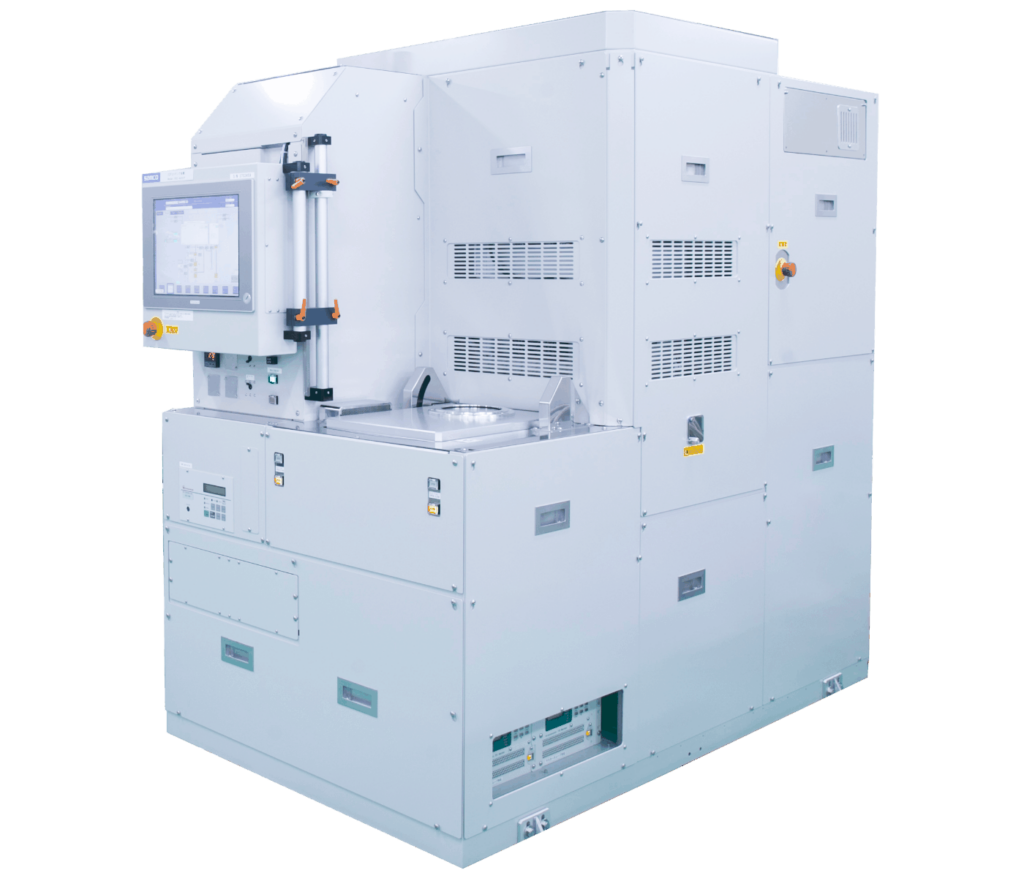
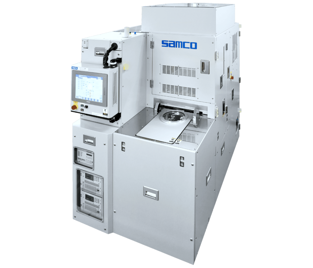
Atomic Layer Etching (ALE) is a technology that separates the adsorption and reaction steps in the etching process and repeats each step to control etching depth at the nano-level. ALE is gaining increasing attention as semiconductor devices become finer, emerging as a key process in the development of next-generation devices. ALE is expected to find applications in processes such as controlling GaN or AlGaN film thickness and maintaining surface smoothness through low-rate etching, as well as in p-GaN/AlGaN high selectivity ratio etching of GaN HEMT device. Samco offers two models of ICP etching systems for ALE, “RIE-400iP-ALE” and “RIE-800iP-ALE,” which are suitable for use across research and production stages.
ALE System Lineup
Key Features & Benefits
- Precise depth control
- Robust, fast-switching gas input valve
- New ICP Source “HSTC™: Hyper Symmetrical Tornado Coil
- High flow exhaust
- Endpoint monitoring
Applications
- Recess etching for GaN HEMT
- p-GaN/AlGaN high selectivity ratio etching
- 2D materials etching
- Photonic crystal etching
- Low rate and low damage etching