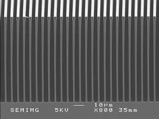
A deep silicon structure with a width of 3 μm and a depth of 70 μm was achieved using the Bosch process on the RIE-400iPB system. This process attained a silicon-to-resist selectivity of approximately 100:1, enabling precise high-aspect-ratio etching for research and microfabrication applications.
Photo courtesy of Yamagata Research Institute of Technology