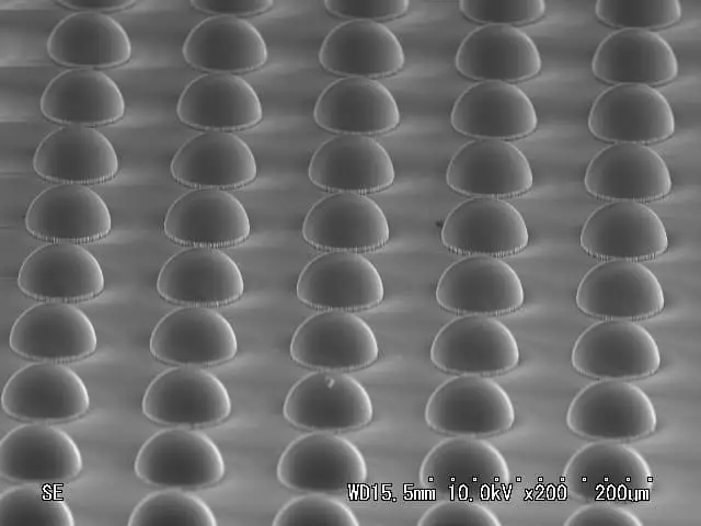
TEOS-SiO₂ deposition for microlens array fabrication with cathode PECVD
This process demonstrates the formation of a microlens array using cathode-coupled PECVD. A layer of P- and B-doped SiO2 was deposited on an SiO2 substrate using LSCVD® equipment, followed by ICP etching to shape the layer into a cylindrical form. The microlens structure was completed through reflow in the 900–1150°C range. Parameters such as etching conditions, film thickness, and reflow temperature enable precise control of lens curvature, meeting the demands of high-precision optical applications.
Photo courtesy of National Institute of Advanced Industrial Science and Technology
