Deep Silicon Trench/Via Hole Etching using Bosch Process

 SAMCO Inc. > Tech Resources > Si Etching (DRIE)

The Bosch Process for Deep Silicon Etching

The Bosch Process is a deep silicon etching technology, which repeats the cycle of isotropic etching followed by protection film deposition. The SF6 plasma cycle etches silicon, and the C4F8 plasma cycle creates a protection layer.

Since the Bosch process has made structures/patterns with high-aspect ratio possible, this process is one of the most revolutionary processes in the history of semiconductor processing technologies.  Nowadays, the process is well known as the name of deep-reactive-ion-etching (DRIE), and it is used for micro-electro-mechanical-systems (MEMS) device fabrication and through-silicon via (TSV) processing.

  • Bosch DRIE 1
  • Bosch DRIE 2
  • Bosch DRIE 3
  • Bosch DRIE 4
  • Bosch DRIE 5
  • Bosch DRIE 6
  • Bosch DRIE 7
  • Bosch DRIE8
  • Bosch DRIE 9
  • Bosch DRIE 10
  • Bosch DRIE 11

SAMCO has developed deep silicon etching process solutions using the Bosch Process.
· Smooth Sidewalls Process (less than 5 nm Scallop Size)
· Ultra Deep Tapered Etching (400µm deep)
· High Etch Rate (over 55 µm/min)
· Tilt Free Process
· High Aspect Ratio (over 40)
· Notch Free Silicon On Insulator (SOI) Etching

For the detail on SAMCO’s DRIE process technologies, please visit Featured Solutions Page.

Deep Silicon Etching for MEMS Device Fabrication

SOI Capacitive Accelerometer

Comb-shape arrays with nanoscale-gap were fabricated for a MEMS capacitive accelerometer.
The etched profile showed vertical scallop-free sidewalls.

Etch Depth : 4.5 µm
Pattern Width : 0.3 µm
Aspect Ratio : 15

Photo courtesy of Tabata/Tsuchiya Lab, Kyoto University

SOI Capacitive Accelerometer

MEMS Liquid Chromatography (LC) Microchip

30 µm deep pillars with different sizes and densities were fabricated.
The pillar distribution worked for fast analysis time under high flow rate condition.

Photo courtesy of Shoji Lab, Waseda University

MEMS Microchip Array

MEMS Optical Chopper

A 15 µm thick silicon layer on a silicon-on-glass (SOG) substrate was etched using the Bosch Process.

The standard Bosch Process causes undesirable notching at the silicon/insulation interface due to electrical charging. SAMCO offers a notch-free SOI etching process that maintains the etch selectivity by using superimposed Radio Frequency (RF) power. The process minimized the notching on the SOG substrate.

Photo courtesy of Tabata/Tsuchiya Lab, Kyoto University

Notch Free SOI etching for MEMS device

MEMS Field Effect Transistor

MEMS structures were fabricated using the Bosch Process to integrate field-effect transistor (FET) with single-walled carbon nanotubes (SWCNTs).
Terminals (source, drain and gate) were separated with sub-micron gaps by the anisotropic etch process.

Photo courtesy of Tabata/Tsuchiya Lab, Kyoto University

FET device fabrication using the Bosch process

Large-area, Flat Bottom Etching

2 mm wide large-area etching was performed using the Bosch Process.
Etch Depth : 300 μm
Etch Selectivity : 170 (over photoresist)
Open Area : less than 10%

The etched profile showed smooth sidewalls and flat bottom without any grasses and pits.

Large Area, Flat Bottom Etching

This etch process is applicable to the fabrication of piezoelectric MEMS sensors, which require a large-area air gap to release a piezoelectric membrane or cantilever by etching.

Deep Silicon Etching for TSV Via Hole Fabrication

There are several requirements in via hole etching for TSV.

1. No undercut below the mask at the upper and wide edge of the TSV
Undercut prevents insulation layer deposition on sidewalls.
2. Smooth and tapered sidewalls
Rough sidewalls deteriorate step coverage of diffusion barrier and copper seed layers by sputtering.
3. Scallop size reduction
Leakage is caused by copper plug peeling or delamination.
4. Rounded corner on the hole bottom
Rounded profile is preferred to prevent breakdown with the concentration of electric fields on the bottom.

SAMCO’s silicon DRIE technologies are applicable to deep via hole fabrication for advanced 3D IC integration. Deep holes with control profile from vertical to tapered can be fabricated without the undercut. Furthermore, the profile has smooth sidewalls using SAMCO’s unique technique of reducing scallop size, and it will lead to improve TSV performance and reliability by reducing resistance and signal loss.

silicon etching for TSV processing
DRIE for TSV

Hole Diameter : Ø30 µm
Etch Depth : 60 μm

silicon etching for TSV processing

Hole Diameter : Ø5 µm
Etch Depth : 50 μm

Deep Silicon Etching for Pillar Fabrication

Pillar fabrication is one of the interesting applications of silicon DRIE technology.
The process is applicable to various devices including microfluidics and optical MEMS devices.

silicon pillar fabrication using the Bosch Process

Pillar Diameter : Ø10 µm
Pillar Height : 20 µm
Sidewall Scallop Width : less than 100 nm
Photo courtesy of Princeton University

Silicon Pillar Formation

250 µm deep vertical pillars (10 µm diameter) in hole patterns
Photo courtesy of Kyushu Institute of Technology

silicon pillar formation

Pillar Diameter : Ø5 µm
Pillar Height : 250 µm
Photo courtesy of Princeton University

Square-shape pillars of 28 μm width were fabricated using the Bosch Process.
The pillars showed square shape from the top to bottom.

Pillar Height : 450 μm
Profile Angle : 89.9°

Photo courtesy of National Taiwan University

silicon pillar formation using the Bosch Process
silicon square pillar (bottom)
Nanoscale Silicon Pillars

Pillar Height : 5 µm
Square Pattern Width : 250 nm
Photo courtesy of National Taiwan University

Silicon Nanoscale Pillar Fabrication

Cubic Head Pillars
Pillar Height : 4.4 µm
Square Pattern Width : 180 nm
Aspect Ratio : 25
Photo courtesy of National Taiwan University

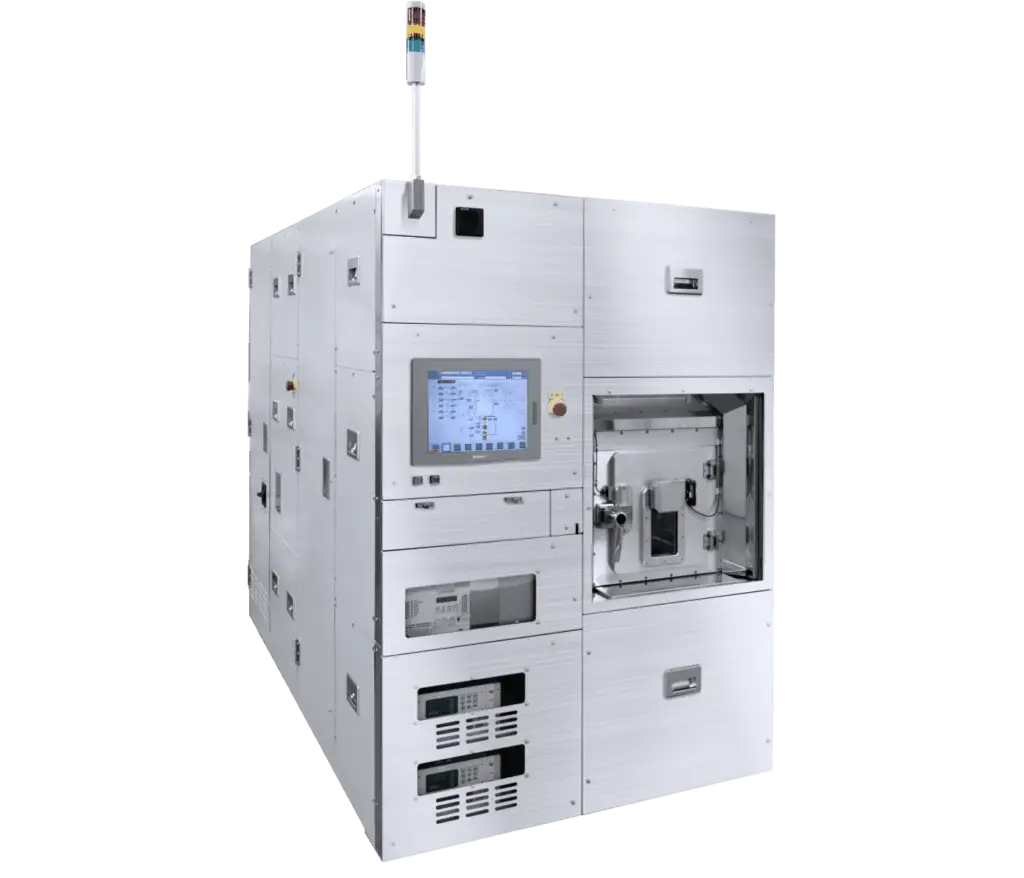
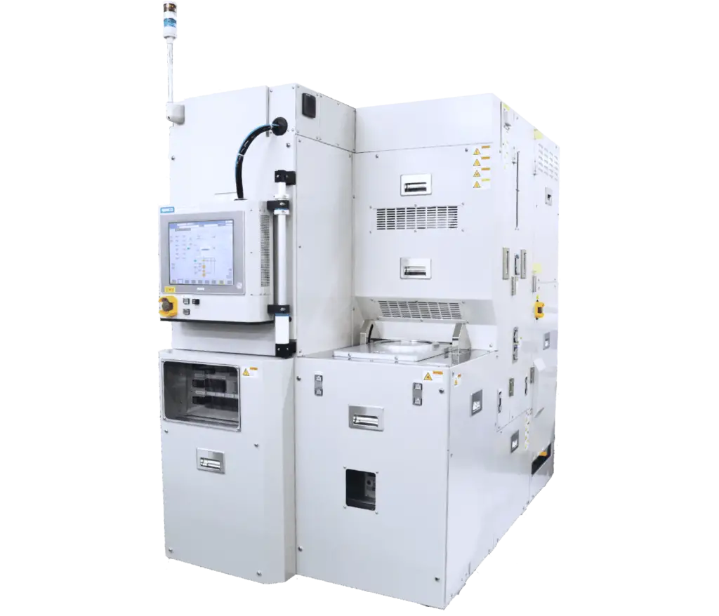
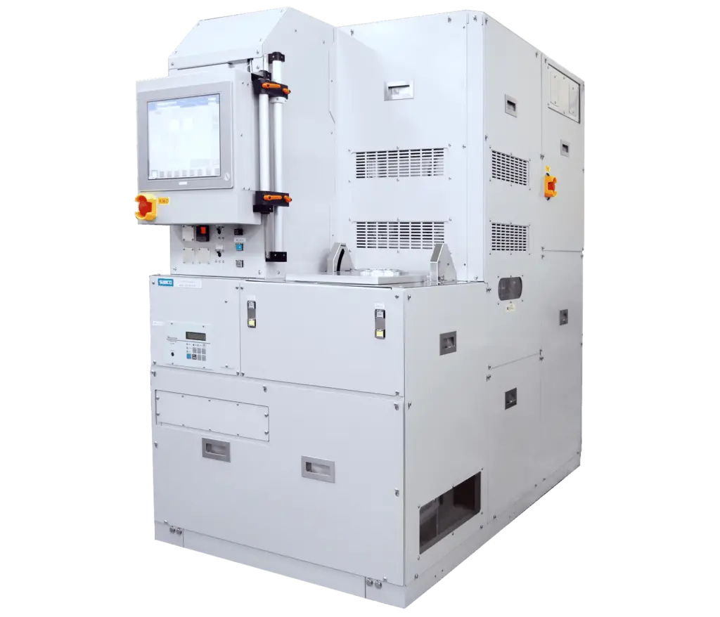
System Lineup for Deep Silicon Etching

DRIE Systems

– Single or Multi-chamber systems for R&D and production
– Optional SiO2 etch kit
– Optional optical/Interferometric end-point detection


Silicon DRIE System


View DRIE Systems >

  • SAMCO Production DRIE System

Testimonial

 SAMCO’s silicon DRIE technologies are used for device fabrication at state-of-the-art nanofabrication facilities including

National Taiwan University

Any Questions?

Contact SAMCO for more product information