
Samco’s etching systems are designed for precise material removal and surface treatment by introducing reactive gases and generating plasma for targeted etching reactions on semiconductor substrates. Our lineup includes advanced Atomic Layer Etching (ALE) for nano-level control, Inductively Coupled Plasma (ICP) etching for high-density plasma etching of III-V compounds and other materials, and Silicon Deep Reactive Ion Etching (DRIE) optimized for MEMS and TSV applications. Additional options, including Reactive Ion Etching (RIE) and Xenon Difluoride (XeF₂) etching systems, support both R&D and high-throughput production with flexibility in handling various substrates and film types.
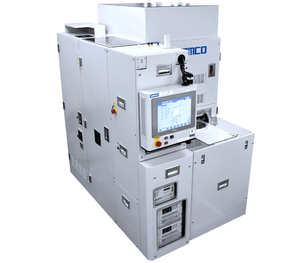
Atomic Layer Etching (ALE) is a technology that separates the adsorption and reaction steps in the etching process and repeats each step to control etching depth at the nano-level. ALE is gaining increasing attention as semiconductor devices become finer, emerging as a key process in the development of next-generation devices. ALE is expected to find applications in processes such as controlling GaN or AlGaN film thickness and maintaining surface smoothness through low-rate etching, as well as in p-GaN/AlGaN high selectivity ratio etching of GaN HEMT device. Samco offers two models of ICP etching systems for ALE, “RIE-400iP-ALE” and “RIE-800iP-ALE,” which are suitable for use across research and production stages.
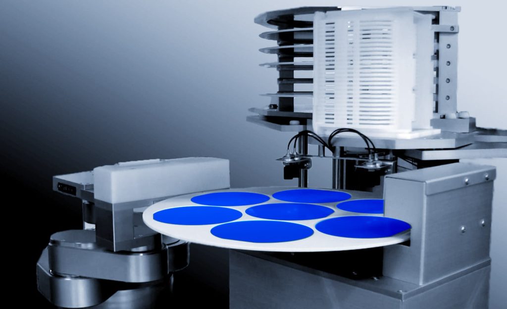
Samco’s Inductively Coupled Plasma (ICP) etching systems deliver high-density plasma solutions tailored to meet the unique process requirements of both research and production environments. Our reliable, durable and compact ICP etching systems allows you to handle a variety of materials including III-V compound semiconductors (GaN, GaAs, InP), silicon, SiC, quartz, glass, dielectrics, and metals.
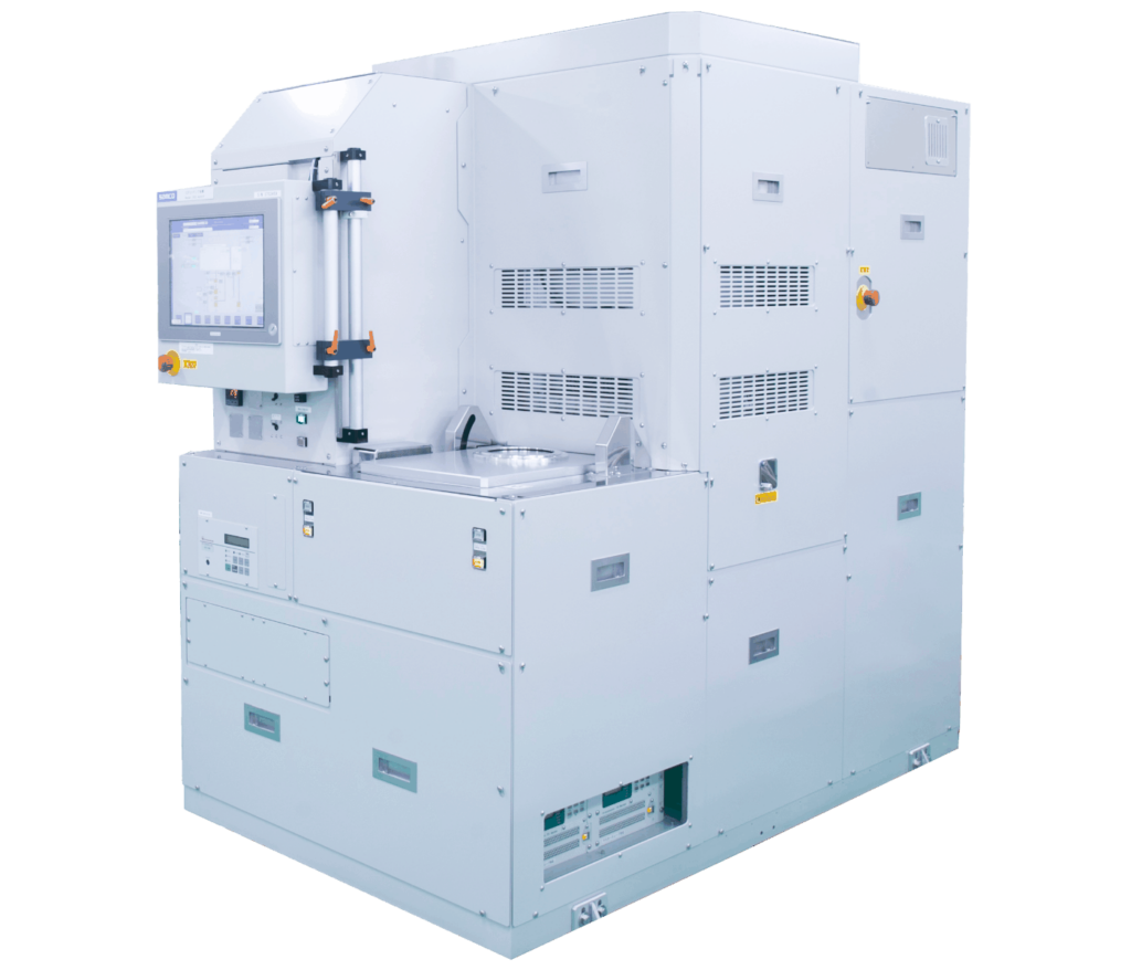
Samco was the first Japanese semiconductor process equipment manufacturer to provide Silicon Deep Reactive Ion Etching (DRIE) systems using the Bosch Process. We offer DRIE systems with a range of sample sizes and number of chambers for MEMS device fabrication and TSV via-hole etching. Our systems have industry-leading process capabilities, and the product lineup covers both R&D and production. For high-volume device manufacturing, a double reaction chamber specification is also available.
Samco offers reliable and durable Reactive Ion Etching (RIE) systems for R&D and production customers. Our benchtop compact RIE etcher is a suitable tool for academic device research and die deprocessing for IC failure analysis. Samco’s open load RIE systems and load lock RIE systems have a wide process window for plasma etching of various materials (silicon, dielectrics, compound semiconductors, metals, polymers and photoresist). The cassette loading RIE systems improve process throughput for device fabrication.
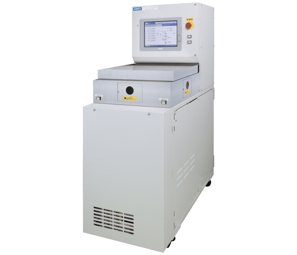
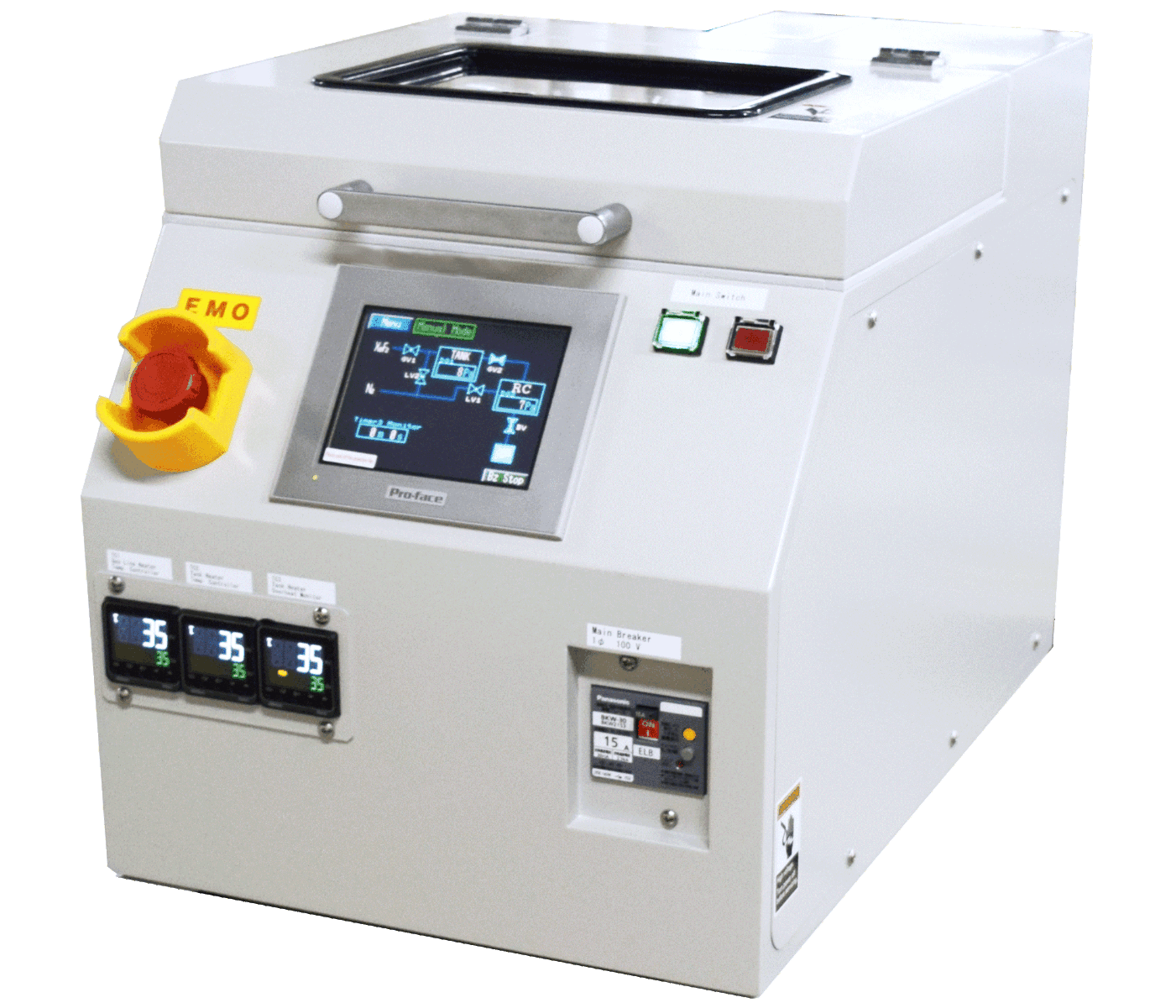
Samco’s Xenon difluoride (XeF2) Etching System is mainly using for the etching of the Si sacrificial layer for fabrication of MEMS (Micro Electro Mechanical Systems) devices. This dry process avoids the destruction of devices due to stiction, which is a problem in the wet process, and eliminates the need for pretreatment and post-processing in the wet process. As a tabletop type system, VPE-4F offers a convenient and compact design.