Introduction
One example of a 4H-SiC power device is the MOSFET (Metal Oxide Semiconductor Field Effect Transistor). While planar MOSFETs have been developed in the past, trench-type MOSFETs have attracted attention to meet demands for high efficiency, such as “low on-resistance.” Samco has been working on trench processing using ICP etching equipment, which is essential for the fabrication of trench-type SiC MOSFETs. In this report, we will introduce the latest trench etching process using ø6-inch SiC wafers, which are currently the standard.
Experiments and Results
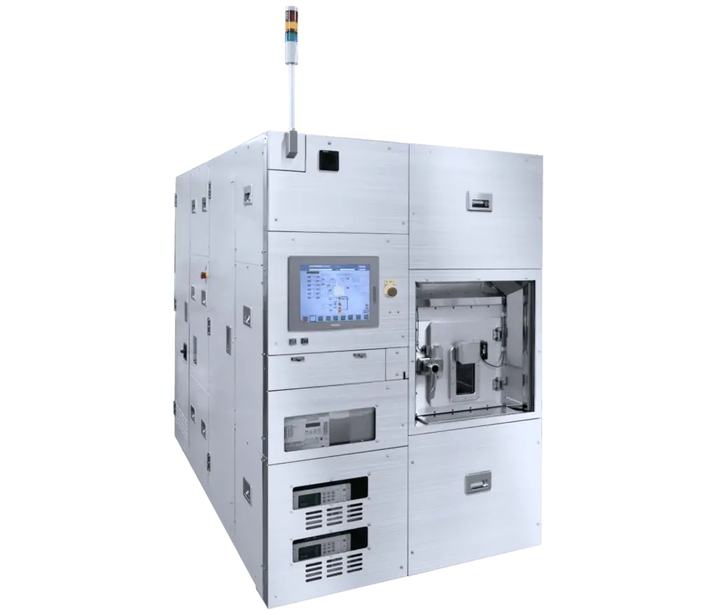
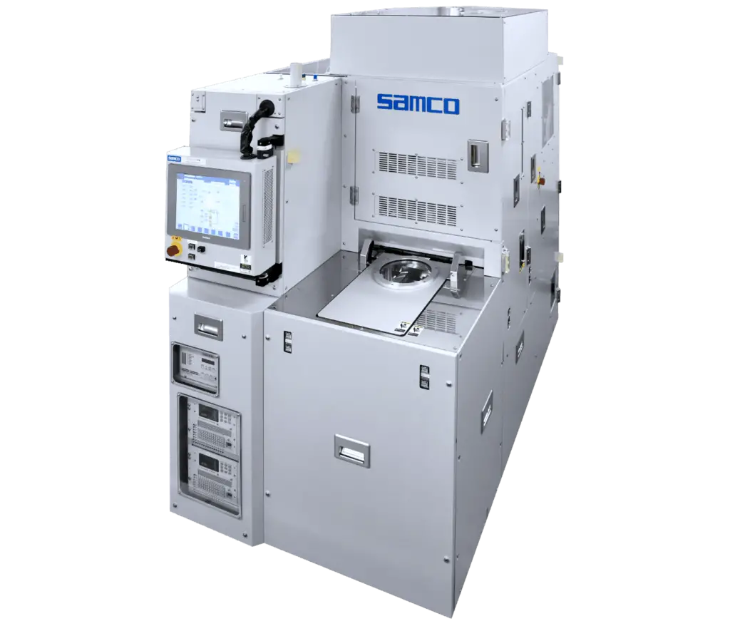
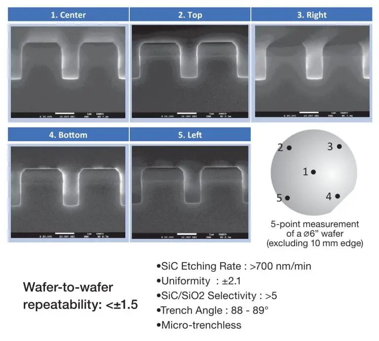
Three key factors in SiC trench etching are achieving a high etching rate, controlling the trench shape, and forming a round shape at the trench bottom. To satisfy these criteria, experiments were performed using Samco ICP etching equipment “RIE-800iP/800iPC” on ⌀6-inch wafers.
Figure 1 presents an example of vertically etched trench patterns with an approximate opening width of 1 mm. The etching rate exceeded 700 nm/min, with a mask selectivity ratio of above 5 (SiC to SiO2), sidewall angles of 88 to 89°, and etching depth uniformity below ±3%. These results mark a significant improvement over the previous etching rate of 450 nm/min, increasing by more than 1.5 times via process optimization. Despite constraints, such as reduced mask selectivity, further adjustments have enabled the etching rate to reach approximately 850 nm/min. The capability to form trenches with opening widths between 0.8 mm and 2.0 mm allows for the processing of even finer patterns.
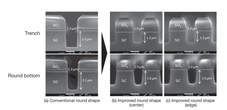
Furthermore, optimizing the trench shape and ensuring a rounded trench bottom is critical. In trench structures, the application of gate voltage can concentrate the electric field at the trench bottom corners, potentially compromising the integrity of the gate insulation film. Therefore, forming a round shape at the trench bottom is crucial. Traditionally, this shape has been achieved through high-temperature annealing; however, there is a growing preference for using dry etching techniques. We have developed a dry etching process to achieve this rounded shape. The optimized conditions produce a uniform round shape throughout the trench bottom. Figure 2 illustrates the outcomes. Figure 2 (a) shows results using conventional conditions, where rounding is confined to the trench corners. Figures 2 (b) and (c) display the results from etching at the center and edge of a ⌀6-inch wafer with the new conditions, achieving an etch depth uniformity of below ±3%. This process maintains consistent trench shapes and reduces variations, leading to favorable results.
Conclusion
This report presents the recent advancements in SiC trench etching processes essential for producing trench-type SiC MOSFETs. The etching rate has increased by 1.5 times, reaching 700 nm/min, while achieving improved control and uniformity of the rounded trench shape. Although the results discussed are based on ⌀6-inch wafers, process development for ⌀8-inch wafers are currently in progress. Moreover, Samco has substantial process data and expertise in gate insulation film deposition (using CVD and ALD) and electrode processing necessary for trench-type SiC MOSFET fabrication. We also specialize in processing and film formation for a range of wide-bandgap semiconductors, including GaN and Ga2O3, thereby advancing the power device sector towards a more sustainable future.