Prof. Yasutaka Matsuo
Professor, Nanotechnology and DX Center, Institute of Electronic Science, Hokkaido University
In this interview, we visit the Research Institute of Electronic Science, Hokkaido University, and talk with Prof. Yasutaka Matsuo about his research on nano, micro-fabrication technology and materials development at the interface.
Brief History
Mar. 1996
Osaka University, Graduate School of Engineering, Bachelor’s Program (Bachelor of Engineering)
Mar. 2001
Hokkaido University, Graduate School of Engineering, Doctoral Program (Doctor of Engineering)
Apr. 2001 – Sep. 2003
Researcher, Science and Technology Promotion Organization
Oct. 2003 – Mar. 2004
Researcher, Hokkaido University
Apr. 2004 – Jul. 2004
Postdoctoral Research Fellowship, Japan Society for the Promotion of Science
Aug. 2004 – Mar. 2007
Assistant, Hokkaido University, Research Institute for Electronic Science
Apr. 2007 – Dec. 2010
Assistant Professor, Hokkaido University, Research Institute for Electronic Science
Jan. 2010 – Mar. 2018
Associate Professor, Hokkaido University, Research Institute for Electronic Science
Apr. 2018 – Present
Professor, Hokkaido University, Research Institute for Electronic Science
Please introduce your current research.
We use microfabrication technology to create microstructures, for instance, micro pillars and pores, on the surface of diverse materials, facilitating specific functionalities. A notable example is the ongoing research in collaboration with Prof. Hirai from Chitose Institute of Science and Technology, where the study is centered around the manipulation of friction by introducing these microstructures to rubber surfaces. Such techniques show potential in inhibiting snow accumulation on structures such as signals and building facades, a common issue in snow prone areas like Hokkaido. The primary emphasis currently lies in manufacturing devices with shape-controlled surfaces and their integration into innovative analytical chips. Additionally, as a part of the Advanced Research Infrastructure for Materials and nanotechnology (ARIM) initiatives, endorsed by the Ministry of Education, Culture, Sports, Science and Technology (MEXT), this team undertakes the responsibility of facilitating users who operate the communal equipment in the clean room of the CRIS – Creative Research Institution of Hokkaido University.
Please tell us how you started your research and how it has developed up to the present.
Originating from the Kansai region of Japan, my academic pursuit in the Department of Applied Physics at Osaka University, recognized for its focus on the study of light, began. A fascination for light studies using lasers led me to the laboratory of Prof. Hiroshi Masuhara, who has since become my mentor. In the Masuhara laboratory, experiments on the movements of electrons within organic molecules under laser light irradiation were conducted.
After completion of my master’s program, a temporary transition to the corporate world occurred, only to be followed by a return to academia, sparked by conversations with Prof. Masuhara. A new opportunity presented itself in the form of an invitation from Prof. Keiji Sasaki, an assistant professor at the Masuhara Lab, who was establishing a new laboratory at Hokkaido University. Consequently, a move to Hokkaido, a region previously unknown to me, took place, bringing its unique set of challenges. The recollection of the entrance examination day for my doctoral program remains vibrant, chiefly due to the snowfall that painted the exterior landscape white. My stint at the Sasaki Laboratory centered around microspectroscopy, a technique used for spectroscopic analysis within microscopic regions.

Following the culmination of my doctoral studies, I secured a postdoctoral fellowship in Professor Kuniharu Ijiro’s laboratory at the Research Institute for Electronic Science. The primary focus of Professor Ijiro’s work was the development of highly functional materials achieved through the accurate organization of biomolecules at interfaces. The research was predicated on a phenomenon: the formation of a monolayer film on water, exploiting the attributes of amphiphilic molecules comprising both hydrophilic and hydrophobic groups. It raised a compelling question: Would the analytical approach to biomolecules alter if their arrangement, structure, or the attachment of electrodes were varied? In this context, I was introduced to the microfabrication technology employed in semiconductors, a technology facilitating the creation of irregular, non-flat substrates to govern the configuration of biomolecules. At that time, due to the absence of a clean room at Hokkaido University, other universities’ laboratories were requisitioned for our microstructure processing. The research focus gradually transitioned from the organization of molecules to the development of unique interfaces using microfabrication and auxiliary methods.
In November 2003, the Hokkaido University witnessed a significant development with the completion of the CRIS Research Building, which incorporated a state-of-the-art cleanroom. This clean room came equipped with advanced tools like electron beam lithography, Samco’s CVD, and dry etching equipment. At the outset, the potential impact of microfabrication on the ongoing research was not entirely evident. However, with the expansion of equipment accessibility and enhancement of processing and analysis capabilities, microfabrication gradually assumed a more pivotal role in the research conducted. This was substantially influenced by knowledge gleaned from other professors at the Hokkaido University who are proficient in microfabrication techniques.
In 2007, the Creative Research Institution (CRIS) of Hokkaido University joined the Nanotechnology Network, now succeeded by ARIM through the Nanotechnology Platform Project of the MEXT. Subsequent to this development, the responsibility of supporting device fabrication for researchers in various companies and universities was conferred upon the writer. This appointment also marked the beginning of my focused work on microfabrication and structural analysis.
While overseeing nanotechnology projects, a collaboration was undertaken with Prof. Masatsugu Shimomura and other researchers in the domain of biomimetics, also referred to as biomimetic technology. This field procures inspiration from the distinctive structures and functions inherent to nature. These unique attributes are replicated and employed in the creation of novel technologies. Prime instances of this include the water repellency characteristic of lotus leaves and the adsorption properties displayed by gecko feet. The surface of lotus leaves possesses a certain texture that repels water. Conversely, geckos have the ability to ascend smooth, vertical surfaces. This is a consequence of van der Waals forces operating between molecules, which is a direct result of the architecture of the numerous microscopic hairs on their feet. The research is concentrated on the physicochemical properties of these structures and aims to utilize a range of materials to duplicate the functions of water repellency and adhesion by employing microfabrication techniques and surface energy control.
What led to the implementation of the Atomic Layer Deposition (ALD) system?
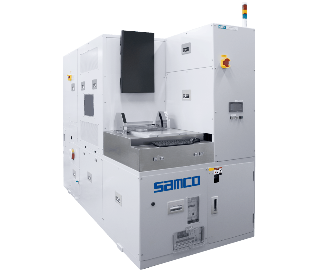
In 2011, the ALD system was introduced by Prof. Hiroaki Misawa at the Research Institute for Electronic Science. Prof. Misawa believed the ALD system would provide valuable contributions to research in photochemistry. Since I was originally involved in photochemistry, I supported the introduction of the system. At that juncture, Samco did not offer ALD systems, which necessitated procuring a system from a reputable Finnish manufacturer. Prof. Misawa was engaged in research aiming to actualize an artificial photosynthesis system via localized plasmons, entities capable of temporarily gathering light. Through the formation of gold nanoparticles on an oxide semiconductor substrate such as titanium dioxide, exhibiting plasmon resonance, light can be used to induce an electrical separation of water into hydrogen and oxygen. Prior to this, single-crystal substrates were exclusively used for managing thin films of titanium dioxide. However, the high costs of single-crystal substrates and the difficulty of fabricating thin films compatible with the structure led to the decision to install an ALD system. The goal was to investigate oxide semiconductors and their structures, especially as TiO2 was infrequently found in films deposited by ALD systems at other Nanotechnology Network Centers in Japan. It was observed that SiO2, Al2O3, and HfO2 were primarily deposited at other institutions.
Following the introduction of the ALD system, support has been extended to a diverse user base due to its availability at the shared the CRIS Research Building facility. Requests were received from lens and optical equipment manufacturers for the utilization of TiO2 in dielectric multilayer films. In a particular instance, a multilayer film with a thickness approaching 300 nm was deposited, resulting in a high-k dielectric film.
What were the reasons for the installation of Samco’s equipment, and what are the opinions of it?
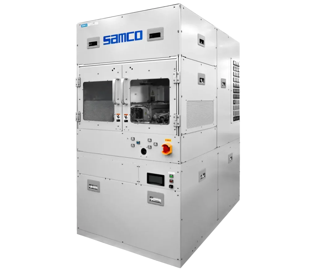
Hokkaido University operates two thermal ALD systems, which are utilized by numerous researchers and engineers from various universities and companies.
This usage trend can be attributed to the fact that these systems permit users to bring their unique deposition precursors.
Upon disclosure of this provision, a surge of inquiries was received, and with the successful implementation of the systems, there was an observable increase in the variety of film types that could be deposited. Concurrently, a demand was noticed for the deposition of films at lower temperatures, necessitating the consideration of plasma-enhanced ALD as an alternative to thermal methods.
As considerations were made for the introduction of a new plasma-enhanced ALD system, the benefits of using novel organometallic precursors became apparent. Previously, difficulties were encountered with reaction chambers when a diverse range of precursors was employed.
Therefore, the introduction of an equipment capable of replacing the reaction chamber was proposed, ensuring its reusability even after becoming dirty during film deposition through a thorough cleaning process. It was deemed essential to ascertain the speed at which a company could respond to these challenges.
Unfortunately, no ALD equipment manufacturer seemed to offer this combination of features. Therefore, when a search was made for a company capable of customizing equipment and providing adequate support, Samco was contacted.
Samco positively responded to this request by not only replacing the reaction chamber but also integrating a feature to vaporize and introduce organometallic precursors by bubbling. There is significant appreciation for Samco’s contribution and high satisfaction with the swift response time demonstrated by the company.

Could you tell us what you keep in mind in your daily research?
The approach taken seeks to “broaden interests.” Upon reflection, participation has spanned various fields, commencing with photochemistry research, transitioning to the study of biomaterial systems, regenerative medicine, cells, among others, and currently focusing on microfabrication technology. Engaging in research across different fields allowed the leveraging of knowledge and experiences from diverse areas, while recognizing shared phenomena and commonalities. Although it is imperative to delve deeply into a singular field, the value of undertaking research that straddles multiple disciplines is equally emphasized.
Encouragement is extended to students to cultivate diverse interests. It remains unpredictable what may prove beneficial in life, thereby increasing the chances of idea generation. Furthermore, undertaking interdisciplinary research expands one’s network of connections. Establishing associations with professors from disparate academic societies, along with individuals from an array of companies, is viewed as significant.
How do you spend your holidays?
Although without any hobbies, I always cook for my family on my days off. Despite not being a particularly accomplished cook, preparing a variety of dishes, such as fried foods and gratins, for the children’s lunches or meals demanding extensive time and effort, is undertaken mainly due to personal preferences. In the beginning, my wife pointed out the lack of an effective clean-up process. Lately, considerations about arrangements and clean-up procedures during cooking have drawn parallels with conducting experiments.
This similarity lies in deciding the quantity of food, determining the procedure, and finally planning the clean-up. Known assistant professors and secretaries opine that cooking and baking are scientific activities. Nonetheless, cooking is often executed at a leisurely pace without stringent adherence to these principles.
Any final words for Samco?
When Prof. Misawa retired, he said, “In conducting research, there are times when ideas alone are not enough to compete. You need a weapon to realize your ideas. That weapon could be a special analysis, a device that allows special processing, or any number of other things”. I believe that Samco is a manufacturer that gives researchers the special tools to help them. During my academic years, I often sought customized products and specialized equipment from manufacturers. As time advanced, the size of research equipment escalated, and the pool of manufacturers receptive to customization requests seemed to dwindle. Despite this, Samco’s ALD equipment has proven responsive, sincerely engaging with our needs and addressing complex challenges. Through their efforts, we can now deposit films previously beyond our capabilities.
It would be commendable if Samco continues to incorporate our needs, as well as those of other users, into their product development.
Thank you very much for taking time out of your busy schedule to speak with us.