Masataka HIGASHIWAKI, Ph.D.
Professor, Department of Physics and Electronics, Graduate School of Engineering, Osaka Metropolitan University (Osaka, Japan)
We spoke with Dr. Masataka Higashiwaki about his research on Ga₂O₃ power and RF devices. He discussed the material’s unique properties, advancements in device development, and challenges in commercialization. Dr. Higashiwaki also shared insights into industry trends, future applications, and the potential impact of Ga₂O₃ technology on next-generation electronics.
Brief History
Mar. 1994
Bachelor of Science (B.S.) in Material Science, Department of Engineering Science, Osaka University
Mar. 1996
Master of Science (M.S.) in Material Science, Graduate School of Engineering Science, Osaka University
Mar. 1998
Doctor of Philosophy (Ph.D.) in Engineering, Graduate School of Engineering Science, Osaka University
Apr. 1998 – Mar 2000
Postdoctoral Researcher of the Japan Society for the Promotion of Science (JSPS)
Apr. 2000 – Sep. 2004
Researcher, Communications Research Laboratory, Ministry of Posts and Telecommunications (reorganized as National Institute of Information and Communications Technology (NICT) in April 2004)
Oct. 2004 – Aug. 2007
Senior Researcher, NICT, Japan
Sep. 2007 – Mar. 2010
Project Scientist, Department of Electrical and Computer Engineering, University of California, Santa Barbara (UCSB) (temporarily transferred from NICT)
Apr. 2010 – Sep. 2012
Senior Researcher, Advanced ICT Research Institute, NICT (returned from UCSB)
Oct. 2012 – Nov. 2013
Chief Senior Researcher, Advanced ICT Research Institute, NICT
Dec. 2013 – Mar. 2021
Director, Green ICT Device Advanced Development Center, Advanced ICT Research Institute, NICT
Apr. 2021 – Mar. 2022
Director, Green ICT Device Laboratory, Koganei Frontier Research Center, Advanced ICT Research Institute, NICT
Apr. 2022 – Present
Director, Green ICT Device Laboratory, Koganei Frontier Research Center, Advanced ICT Research Institute, NICT
(part-time post)
Apr. 2022 – Present
Professor, Department of Physics and Electronics, Graduate School of Engineering, Osaka Metropolitan University
Please introduce your current research.
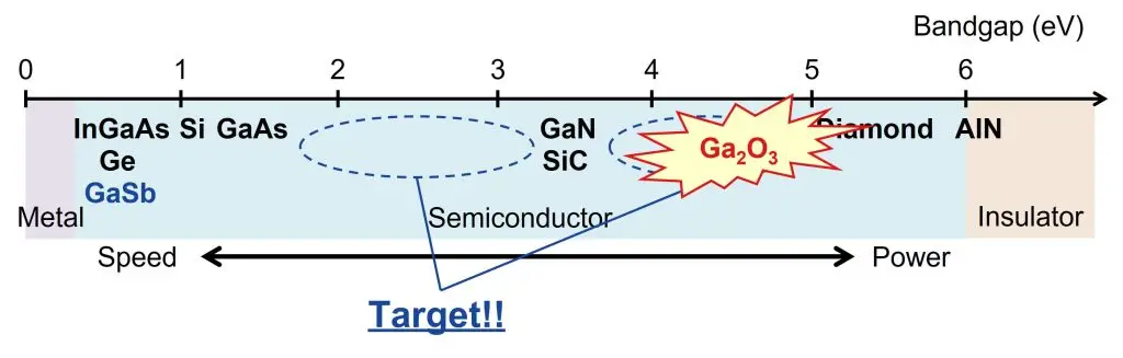
I am involved in research and development on novel functional electronic devices, specifically transistors and diodes, that leverage the exceptional material properties of gallium oxide (Ga2O3), a recently discovered semiconductor. Ga2O3 is distinguished by its substantial band gap of 4.5 eV, surpassing the 3.4 eV of silicon carbide (SiC) and gallium nitride (GaN), both of which have garnered attention as semiconductor materials for next-generation power devices. Ga2O3 exhibits remarkable attributes, including a high breakdown voltage and substantial current conduction capacity. Our research extends to the application of Ga2O3 in devices suitable for use in extreme conditions, such as high-temperature environments, radiation exposure, and corrosive gases. We are collaborating extensively with companies, national research institutions, and universities in Japan and abroad to advance the research and development of Ga2O3-based devices for power electronics and applications in extreme environments.
Please describe how your research journey began and how it has led you to your current position.
During my academic tenure, I studied at the School of Engineering Science, Osaka University. As I entered the realm of laboratory work, my fascination with semiconductors led me to become a part of Prof. Satoshi Hiyamizu’s research group. Prof. Hiyamizu was focused on advancing the growth of GaAs thin films through molecular beam epitaxy (MBE). My educational path culminated with the attainment of a Ph.D., with a research emphasis on GaAs quantum wires. Prof. Hiyamizu’s legacy in the academic community is built on pioneering work, particularly the publication of the first-ever paper on GaAs high electron mobility transistors (HEMTs), a collaborative effort with Emeritus Fellow Dr. Takashi Mimura from Fujitsu Laboratories. It was Dr. Mimura who conceptualized HEMTs and enlisted Prof. Hiyamizu’s MBE expertise to grow GaAs thin films, bringing their vision to fruition.
This connection paved the way for my training at Mimura Fellow Group of Fujitsu Laboratories after I completed my doctoral program at Prof. Hiyamizu’s Laboratory. My academic pursuits at the university primarily revolved around materials, while my tenure at Fujitsu Labs provided valuable insights into device processes, particularly in the realm of InP-based HEMT research. A year and a half later, my academic journey led me to the Communications Research Laboratory (CRL), now a part of the National Institute of Information and Communications Technology (NICT), where I assumed the role of a researcher in April 2000.
Since I could choose my research theme relatively freely at CRL, I started research on the development of InN FETs for wireless communication systems beyond InP HEMTs. This proved to be an ambitious undertaking, and, within two and a half years, we made significant progress, successfully growing high-quality crystals through MBE. However, the research landscape took an unexpected turn when it was revealed that the band gap of InN, theoretically calculated at 1.9 eV, was in fact only 0.6 eV.
Driven by a relentless determination to excel in my upcoming research endeavor, I opted for GaN HEMTs designed for millimeter-wave applications, a relatively unexplored area at the time. Millimeter waves are characterized by wavelengths ranging from 1 to 10 mm and frequencies spanning from 30 to 300 GHz. At the time, the performance limitations of high-frequency GaN HEMTs were typically around 30 GHz, and there was a prevailing perception that GaN was primarily suitable for frequencies below this threshold. However, our understanding of GaN’s physical properties indicated the potential for use up to 100 GHz, paving the way for a research journey that unfolded rather smoothly, culminating in the demonstration of impressive device performance.
One critical performance metric in the realm of high-frequency transistors is the current gain cutoff frequency (fT), which signifies the highest operable frequency. As a rule of thumb, the actual device can operate at approximately half the fT. In 2002, GaN HEMTs achieved a milestone with the highest recorded fT of 121 GHz. Building upon this, in 2005, we demonstrated an fT of 152 GHz, and after a series of refinements, by 2007, we had reached an unprecedented fT of 190 GHz. It was my belief that further refinements could potentially propel us towards the remarkable goal of 200 GHz.
Fortunately, during that period, I had the chance to move to University of California, Santa Barbara (UCSB), where Prof. Umesh Mishra, renowned for his GaN-based transistor work, was conducting research. I was seconded from NICT to UCSB for a duration of two and a half years. My stint at UCSB offered a valuable opportunity for self-assessment, where I identified areas in need of enhancement and acknowledged my strengths.
One aspect that became evident was my deficiency in the fundamentals of semiconductor physics and devices. While I possessed a rudimentary understanding of semiconductor physics derived from reading books, my experience at UCSB, especially through dedicated coursework, provided me with a comprehensive grasp of the core principles of semiconductor physics.
Conversely, I recognized my strengths in the strategic planning and execution of research, my analytical thinking, and the efficiency of my work. In comparison to researchers in the United States, I came to believe that I excelled in these aspects.
I continued my research on millimeter-wave GaN HEMTs at UCSB. Nevertheless, I encountered a significant challenge: the clean room at UCSB was frequently congested. In addition to students and researchers of UCSB, professionals from neighboring companies also utilized the facility, limiting my access to the equipment. This was in stark contrast to my prior experiences in Japan, where I conducted experiments in the clean room from morning until night. However, my time within the UCSB clean room was restricted to approximately half a day. Consequently, during my spare hours, I engaged in contemplation, pondering the question, “What should be my next research endeavor?” It was during these moments of reflection that I had the opportunity to plan and chart my future research direction.
Notably, I achieved substantial progress in the realm of millimeter-wave GaN HEMT research. My prior achievements in Japan, particularly the attainment of an fT of 190 GHz, had a significant impact in the United States. For instance, approximately a year and a half after my arrival in the U.S., DARPA (Defense Advanced Research Projects Agency) initiated a project dedicated to the research and development of millimeter-wave GaN-based transistors.
When a company or a major organization embarks on research in the same domain as mine, I contemplate transitioning to a new research area. This choice is motivated, in part, by the formidable challenges faced by universities and public research institutions when pitted against the substantial financial investments and human resources allocated by corporations. Furthermore, given my current role at a university, I perceive no imperative to engage in such competition. As a university researcher, my expertise lies in engineering rather than pure physics.
Consequently, I hold the belief that my role concludes when companies undertake full-scale Research and Development (R&D) initiatives and assume responsibility for product development. As a result, I advocate establishing a collaborative relationship. This arrangement entails that, as companies progress to the stage of full-scale R&D, we, as university researchers, transition to new domains and offer fresh ideas to companies once again.
During my tenure at UCSB, I had not yet determined whether I would return to Japan. Nevertheless, given the substantial budget earmarked for the development of millimeter-wave GaN transistors, I recognized the opportune moment to transition to fresh research endeavors and embrace new challenges.
How did you start your research on gallium oxide (Ga2O3) power devices?
Another strength I realized during my time at UCSB is my comprehensive understanding of both materials and devices. In the typical research landscape, material and device researchers often specialize independently. However, I possess expertise in both domains, which prompted me to explore the potential of developing devices using novel semiconductor materials. When I refer to new semiconductor materials, I am specifically alluding to materials with band gaps distinct from those of conventional semiconductors. This distinction is vital because many of a semiconductor’s physical properties are intricately tied to its band gap. As alluded to earlier, my research direction shifted when I discovered that the band gap of InN is 0.6 eV. One of the catalysts for this change was the recognition of other semiconductor materials, such as InGaAs and Ge, sharing the same 0.6 eV band gap. During my examination of Ga2O3 papers, I encountered multiple references to Prof. Shizuo Fujita of Kyoto University (currently serving as an external director of Samco Inc.). This led me to initiate contact with him. At that time, Prof. Fujita was actively exploring the application of Ga2O3 in ultraviolet light-emitting devices, sparking my contemplation: “Could this material also be harnessed for unipolar power devices?”
Subsequently, in 2010, I contemplated rejoining NICT upon my return to Japan with the intention of commencing research on Ga2O3 devices. However, serendipitously, an opportunity arose through Prof. Fujita’s connection with a company actively developing Ga2O3 substrates for collaborative research. The company supplied me with Ga2O3 substrates and epitaxially grown films, entrusting me with the responsibilities of transistor fabrication and evaluation as part of our collaborative research endeavors. While the semiconductor properties of Ga2O3 were well-established, this marked the first instance globally in which a functional transistor had been realized. This groundbreaking achievement acted as a catalyst for the significant upswing in worldwide Ga2O3 device research.
Subsequent significant milestones in Ga2O3 device development encompass advancements in ion implantation doping technology, the creation of transistors and diodes with field plates to enhance breakdown voltage, and the design of vertical transistors structurally better suited for power devices. Recently, we conducted experiments to assess the radiation resistance of Ga2O3 devices, scrutinizing their capacity to maintain operational integrity after exposure to high doses of γ-rays, all while avoiding substantial degradation. In applications within the realms of accelerators and space, γ-ray resistance becomes imperative when cumulative doses approach approximately 100 kGy (kilogray). For nuclear reactor applications, γ-ray resistance exceeding 1 MGy is a prerequisite. Remarkably, the Ga2O3 transistors we fabricated not only functioned effectively following exposure to 1 MGy of γ-ray irradiation but also exhibited no discernible deterioration in their inherent characteristics. This compelling result underscores the potential utility of Ga2O3 devices, extending beyond power electronics applications to include their role as radiation-resistant devices.
What are your future plans for your research?
I would like to advance my research to the point where Ga2O3 devices can be put to practical use. As previously highlighted, it falls under the purview of companies to put these devices into practical applications. My role centers on driving device development to the extent where companies embark on comprehensive research and development endeavors. While some companies have already commenced internal development of Ga2O3 devices, it appears that many of them are currently in a wait-and-see phase. Should these companies take a more resolute step towards the commercialization of Ga2O3devices, I am of the opinion that my role will be 90% accomplished.
I think it is important to note that the vertical Ga2O3 transistor we announced in 2018 is not just a vertical structure, but can also be fabricated using ion implantation doping of Si and nitrogen (N). This is because the ability to fabricate devices using ion implantation, a simple process with a large degree of freedom in structural design, directly leads to improved productivity. I had aspired that the revelation of these findings would invigorate research and development within the industry. However, in practice, our progress is ongoing. Presently, we are actively pursuing advancement in collaboration with other universities and companies, as part of research supported by the Ministry of Internal Affairs and Communications.
Since I shifted my primary role to the university last year, I am earnestly contemplating a renewed endeavor in the future, focusing on the development of novel materials using MBE. My goal is to uncover new semiconductor materials through MBE.
You have experience using Samco's equipment, what are your impressions?
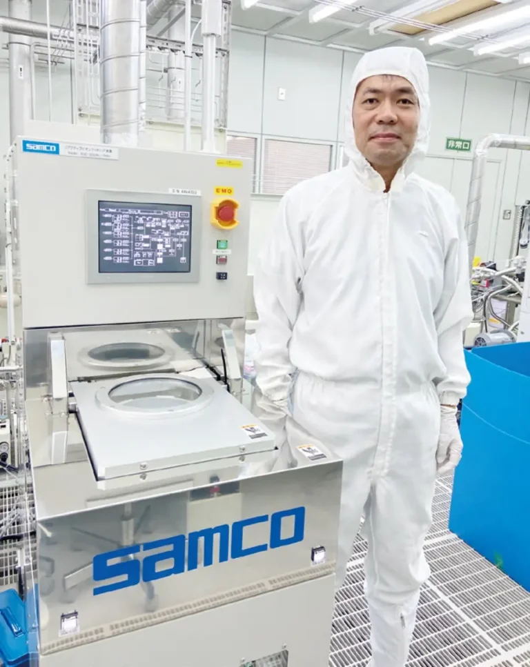
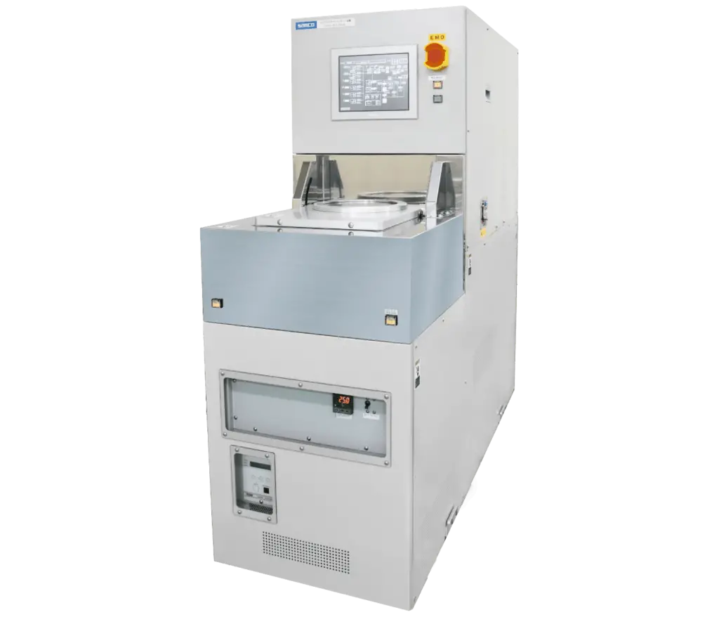
For several years we have been using Samco’s equipment in the clean room at NICT. More recently, we introduced the same RIE equipment, RIE-200NL, at Osaka Metropolitan University. In 2022, we integrated an RIE-200NL tailored for chlorine (Cl) gas systems, and in 2023, we acquired another RIE-200NL designed for fluorine (F) gas systems. The Cl-based RIE system primarily serves the purpose of Ga2O3 etching through the use of BCl3 gas. The upcoming F-based system will be employed for the processing of SiO2 insulating films and ALD-deposited Al2O3. Furthermore, we’ve transitioned the PD-240, which is dedicated to SiO2 deposition, from NICT to the university, albeit it is still in the startup phase. While this tool has surpassed the two-decade mark, Samco’s equipment maintains a remarkable track record of durability, inspiring confidence in its longevity.
What do you keep in mind in your daily research?
I continually underscore the importance of critical thinking to my students. While some individuals advocate immediate action, I stress the significance of thoughtful deliberation followed by purposeful action. I firmly believe that this approach is not only vital in the realm of research but also applicable to various aspects of societal engagement. My guidance often revolves around the following principles: ‘Upon defining a research objective, let us contemplate the means to achieve it, explore possibilities, evaluate alternative approaches, and identify the most promising one.’ Once the choices are made clear, we internalize them and proceed to experiment with the most promising alternatives. Subsequently, we verify the experimental data and, in the event of unexpected outcomes, we analyze their root causes. Through the iterative application of this process, we significantly enhance the probability of achieving success. There’s no definitive categorization of thinking as good or bad, no limit to thinking too much or too little. Engage deeply in your thoughts and endeavor to perform at your best. This is the guidance I consistently provide to my students, always delivered with a gentle and supportive approach.�
As a researcher, I value how satisfied I am with my own research. I employ two distinct criteria for evaluation: the first centers around external assessments. Evaluations provided by peers and institutions are undeniably pivotal for securing research funding and advancing one’s career, and they cannot be overlooked. However, I am not inclined to solely chase external evaluations. The second criterion pertains to self-assessment. For me, the level of personal contentment I draw from my research stands as the most fundamental benchmark. I experienced immense joy when I successfully operated the Ga2O3 transistor for the first time. To be completely honest, I consider it the pinnacle of my research career. Nonetheless, over the next 10 to 20 years, I aspire to embark on one more research project that will bring me profound self-satisfaction.
Finally, I have received valuable guidance and support from many people. My goal is to extend similar support to the younger generation through research and education, without considering it merely as a way to reciprocate. In particular, I am dedicated to ensuring that students within my laboratory can, decades from now, express their contentment by stating, “I am glad to be a part of this laboratory.”
Any final words?
I have the impression that Samco’s equipment is highly durable, stable, and user-friendly. It stands as an exemplary product from a renowned Japanese manufacturer. Furthermore, I am exceptionally content with the outstanding support they provide. As we look to the future, my aspiration is to witness Samco’s innovation in the form of original equipment. Historically, Japanese manufacturers have often followed the lead of U.S. companies in the semiconductor equipment industry. Instead, I wholeheartedly recommend that Samco takes the lead by developing cutting-edge equipment tailored for the global market.�
Consider, for instance, Mist Chemical Vapor Deposition (CVD) equipment. Mist CVD technology is ideal for α-Ga2O3 deposition, a capability I understand Samco has already mastered. However, the distinctive attributes of Mist CVD technology extend beyond this, allowing for the deposition of thicker films compared to ALD, all with excellent coverage even under high-aspect-ratio conditions. This technology holds significant promise for a wide range of applications, including coatings and passivation. Its user-friendly nature and material selectivity further enhance its appeal. Given the versatile film deposition capabilities of Mist CVD, it is poised for applications far beyond Ga2O3. I eagerly expect that Samco will pioneer the world’s first equipment, playing a significant role in the development of next-generation devices.
Thank you very much for taking time out of your busy schedule to speak with us.