Dr. Johann Osmond
NanoCharacterization Lab Head, NanoFabrication Lab Scientific Officer at the Institute of Photonic Sciences (ICFO)
During this interview, we had the opportunity to speak with Dr. Johann Osmond about research being conducted at the Institute of Photonic Sciences, which includes various fields of photonics, such as quantum optics, nanophotonics, biophotonics, nonlinear photonics and more.
Brief History
Sep. 2001
Engineer Degree in Physics, Graduate School of Engineering, Centrale Méditerranée (France)
Sep. 2001 – Apr. 2002
Engineer, Pirelli Labs and Politecnico di Milano Consortium (Italy)
Apr. 2002 – Oct. 2004
Engineer, Pirelli Labs and Bicocca University Consortium (Italy)
Jun. 2008
Completed PhD program in Physics, Politecnico di Milano (Italy)
Jul. 2008 – Sep. 2009
Post-doc Researcher, Institut d’Electronique Fondamentale (France)
Sep. 2009 – Mar. 2022
Staff Researcher, Institute of Photonic Sciences (ICFO) (Spain)
Apr. 2019 – Present
NanoFabrication Lab Scientific Officer, Institute of Photonic Sciences (ICFO)
ICFO is a highly worldwide renowned photonics research institute located in Castelldefels, Spain. Can you tell us a little more about it?
ICFO-The Institute of Photonic Sciences was founded in 2002 by the UPC, The Technical University of Catalonia (Universitat Politècnica de Catalunya · Barcelona Tech – UPC) and CERCA, Research Centers of Catalonia (Centres de Recerca de Catalunya), which is a network of research institutes across the Catalonia region, focusing on a range of topics from photonics, telecommunications, and high energy, to biology and genomics.
Can you tell us about the labs at ICFO, specifically the lab you are the scientific lead for?
My lab was established more than 15 years ago as the Nanophotonics Lab. It started out as a small laboratory, but it eventually grew thanks to the acquisition of new equipment and technology. Today, it is mostly used for nanofabrication in small volumes, for prototyping and for material and structure characterization.
In addition to the Nanofabrication and Nanocharacterization labs facilities, ICFO has several other labs, including the Super-resolution Light Microscopy and Nanoscopy (SLN) facility, the Biology Lab (BIL), the Chemistry Lab (BCL), the Post-Processing (PPL) Lab, all which give support to the researchers to be able to conduct frontier research.
The labs are accessed by all users, usually Master’s, PhD, and postdoc students who can use the tools independently after a proper training of the facilities. We have a team of four people in our lab who give high-level support to all fabrication and characterization processes. My official position is Scientific Officer of the Nanofabrication Lab, and I am also head of the characterization lab.
The various labs cover a wide range of areas, each with different management structures. These labs function as platforms, which give support to the research that is being carried out across different institutes.
Within photonics, what research areas does the ICFO focus on?
The Institute carries out its research in six main areas: Advanced Quantum Materials, Energy and Environment, Quantum Science and Technologies, Bionano and Medical Photonics, Light and Matter, and Ultra-Fast Science. Due to the multidisciplinary nature of the research carried out here, research areas often overlap in terms of areas of applications. So, research groups host scientists from a mix of backgrounds including Physics, Engineering, Biology, Chemistry, Mathematics and Medicine.
Now, the nanofabrication and nanocharacterization lab activities mainly focus on nanophotonics, encompassing a wide array of topics. We support several research groups within nanophotonics, each focusing on different areas. For example, one significant area of application is 2D and Quantum materials. We have a group working on Quantum dots for photo detection and lasers, another group dedicated to carrying out research on solar cells, and a team focused on photovoltaics. There is also a group working on nanomechanics and a newly established group working on Photon-mediated CO2 reduction, that is, they use light to find ways to reduce CO2 in the atmosphere.
Additionally, research on Thermophotovoltaics (TPVs) aims to retrieve energy from heat, functioning in the infrared spectrum. This is one of the applications that we are wanting to do research on using Samco’s CVD system PD-220NL. We also have a group working on nanoplasmonics for biosensing and optical antennas, and another research group that uses our facility to develop nanostructured glass with anti-bacterial or hydrophobic characteristics, achieved by creating nanostructures on the glass.
What are the future prospects of this research?
All of the research carried out at ICFO is aimed at having a significant potential for future applications. Our research spans both basic and applied science, providing a comprehensive range of projects. Some projects are in collaboration with companies, some of which are spin-offs from our own institute, and focused on developing products. Other projects are still at a more fundamental physics research level, and therefore, still require more research to be considered mature enough for any impactful application for society.
Due to my background in integrated photonics, I am interested in our research on PICs (photonic integrated circuits). All the research topics at ICFO are fascinating because they involve hands-on work and practical applications. This summer, I have been more involved in various research projects. The most inspiring projects to me are ones aimed at creating a cleaner planet and a better sustainable future. This really has a significant impact on me and the work I carry out.
What is your personal history in the semiconductor field, and how has it led to where you are today?
My background bridges both the semiconductor and photonics fields. I studied engineering in physics in France at Centrale Méditerranée, focusing on semiconductors, optics, and data processing. In my final year, I participated in an exchange program through the Erasmus Programme, spending a year at Politecnico di Milano (Polimi) in Italy. There, I spent the first semester attending lectures and the second semester on practical applications. This was a fascinating experience, particularly the lectures of Professor Orazio Svelto, renowned for his expertise in lasers.
My practical applications were conducted with a consortium between Polimi and Pirelli, a company whose expertise range from tires to cables and optical communications. They were the first ones to sell EDFA, erbium doped optical fiber amplifiers, back in 1993 marking their foray into optical communications and fiber optics. I completed my final internship for my engineering degree with this consortium.
Following this, I transitioned into materials for optical communication through another consortium between Pirelli and the University of Milano-Bicocca. Eventually, I pursued a Ph.D. at Polimi, working in a laboratory led by Professor Hans von Känel. He invented LEPECVD, a technique for low energy plasma enhanced chemical deposition of silicon germanium. My Ph.D. research focused on using germanium for photodetectors. This technology produced high-quality materials with excellent properties, such as very low dark currents of Ge photodetectors and high hole-mobility in high quality strained Ge channels . I was responsible for fabricating and characterizing the photodetectors.
Additionally, I managed a small clean room facility, gaining my first significant experience in clean room responsibilities. I continued in this role while completing my Ph.D. Later, I undertook a postdoc in Paris, studying similar topics, part of the known such as Group Four Photonics, but characterizing germanium photodetectors fabricated by a facility in France.
In 2009, I joined ICFO as a research engineer focused on process development. For nearly 15 years, my responsibilities have expanded to include, developing new technologies, supporting various research groups and acquiring new equipment. My role encompasses process development, scientific training, and increasing management responsibilities in fabrication and characterization.
From managing a very small clean room, we have grown to oversee around 30 tools for the entire institute. We currently have 80 active users, primarily from the institute, but we are increasingly opening our facilities to local companies and startups. While our main activities remain internal, we also collaborate with companies on specific research topics.
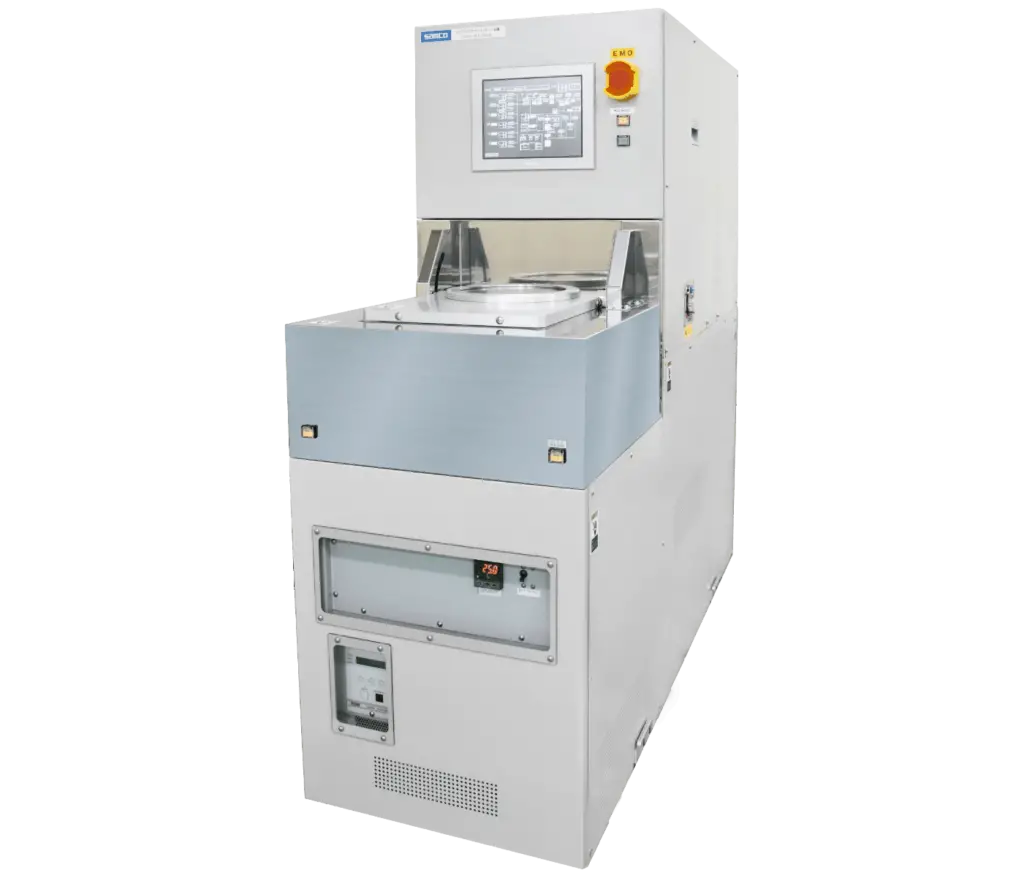
ICFO got their first Samco system (RIE-10NR) in 2018. How has it been utilized?
The system was obtained through an agreement with one of the research groups rather than the facility itself. Initially, it was primarily used by that group for their research, while our facility used it as a backup during maintenance or unavailability of our own systems. Although we had occasional access, the system was mainly dedicated to 2D materials research at that time.
Recently, the system was moved back to the facility and is now one of our three etching systems in use, and thus, the facility took responsibility over its use and management. Now, we aim to complement or divide the usage of the systems for different processes and functions. We are still finalizing the details, but one of the RIE-10NRs main features is its 8-inch capability, which other systems in the lab do not have. We plan to start with 8-inch etching and then divide the usage based on materials. For instance, we might use it for PbS (lead and silver) quantum dot research. This is one example of its potential uses.
What made you decide to get more systems from Samco?
We are very interested in the capabilities that Samco’s systems offer, which other companies do not. Our researchers are satisfied with the performance of Samco’s systems. We are seeking high-quality tools from leading players in the market, and Samco is a strong contender. It would be advantageous to have several tools that complement each other. We are particularly interested in some of the unique functionalities that Samco provides.
Regarding CVD, Samco’s development of liquid sources is more advanced compared to other companies, which is significant for safety reasons. This is a key aspect for us.
Aqua Plasma is another very interesting and innovative tool as well. Currently, we use oxygen plasma, but Aqua Plasma has very interesting features and capabilities that we may explore in the future.
What are some of the most common challenges that ICFO faces with nanofabrication activity applied to research in photonics?
One of the main challenges we have is achieving reproducibility. For any process, results that are consistent are crucial. Additionally, managing the use of many different materials within the same systems poses another challenge. So, due to the variety of activities, it is difficult to provide a solution for all materials without interference. Some materials may not be compatible with others, so it is essential to separate processes to avoid cross-contamination. This is particularly tricky for us because we handle numerous applications with many different materials. It is not like in a company where the same processes and materials are used 24/7. It is quite the opposite, here at our facilities, people want to try everything. Managing this can be quite challenging.
Are you satisfied with your RIE-10NR?
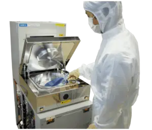
Considering our original arguments for purchasing the RIE-10NR, we are happy with the system overall. At that time, it was very affordable compared to other systems, and had the most compact system design for 8-inch capability. It offers a lot of value and high quality for its low cost of ownership. A very positive aspect of the system is its reliability. It rarely malfunctioned; I think we had only one incident so far, but most of the time it was working fine.
Recently, we moved the tool to a more high-level cleanroom. We managed the entire move by ourselves, disconnecting and transporting it between rooms. Once plugged in, it turned out to work perfectly fine, with the same pumping efficiency and best pressure. We have not done any maintenance since acquiring the system in 2018. It is still working properly, maintaining good vacuum levels, and in good shape.
Before you purchased your RIE-10NR system from Samco, did you have any concerns about doing business with us? What have you learned about Samco’s service, our availability, and so on?
One of our main concerns was about customer service once the machinery was acquired. This was not limited to Samco but was a common concern in Europe with companies in Japan and overseas. We worried about obtaining proper customer service and maintenance without local engineers in Spain. However, the RIE-10NR system is very reliable. Samco’s equipment has many countermeasures in place to prevent breakdowns, something that often occurs with other companies, so I don’t think we had to worry about service in the end.
The fact that there are not as many systems installed in Europe yet was our second concern. However, since Samco has many systems around the world, we were able to get a few references from previous clients, specifically from the US at the time. This made us confident in our purchasing decision.
We have been satisfied with our choice, and communications with Samco are good. The process to buy the system was very short and the support desk is very agile. We can ask any support question, and our Samco representative is always available to answer our technical questions, apart from being very knowledgeable about the system. We are quite happy about this. It is always better when you can talk at a technical level with someone and you see there is a clear understanding on the issues, which helps a lot when answering our questions.
Would you recommend Samco’s products to other people?
Yes, I would. My experience with Samco has primarily been with RIE and ICP-RIE. For these tools, I would definitely recommend them. We conducted extensive demos with the ICP-RIE system RIE-400iP and were pleased with the results, as well as the performance of our RIE-10NR system.
Any final words?
Consider expanding to Europe. I believe there is significant opportunity here. I would be pleased to see more customers nearby that purchase this equipment. During my visit to Kyoto, I had excellent interactions and built good personal relationships. It was a very positive experience.
Thank you very much for taking time out of your busy schedule to talk with us.
Process capabilities of Samco's CCP RIE Systems
Samco’s Capacitively Coupled Plasma (CCP) Reactive Ion Etching (RIE) systems provide precise, low-damage etching solutions for various materials. These systems enable fine patterning, anisotropic etching, and surface treatment for a range of applications.
Key process capabilities include:
- SiO₂ and SiNx Etching – High selectivity and excellent profile control.
- Polymer and Photoresist Removal – Efficient ashing and descum processes.
- GaN, GaAs, and InP Etching – Optimized for III-V compound semiconductors.
- Organic and Polymer Etching – Precise material removal for microfabrication.
These systems are ideal for device fabrication in optoelectronics, MEMS, and semiconductor research.