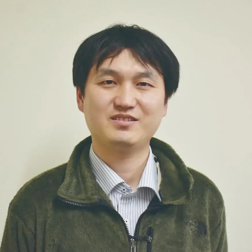
Dr. Hiroto Sekiguchi
Associate Professor, Graduate School of Engineering, Department of Electrical and Electronic Information Engineering, Toyohashi University of Technology
During this interview, we visited Toyohashi University of Technology and had the opportunity to speak with Associate Professor Hiroto Sekiguchi about his research, which includes the development of bio-implantable devices using microLEDs and the development of flexible microLED films.
Brief History
Mar. 2005
Graduated from the Faculty of Science and Technology, Sophia University, with a degree in Electrical and Electronic Engineering.
Mar. 2007
Completed Master’s program in Electrical and Electronic Engineering, Graduate School of Science and Technology, Sophia University
Apr. 2009 – Mar. 2010
Special Research Fellow (DC2) at the Japan Society for the Promotion of Science (JSPS)
Mar. 2010
Completed Doctoral program in Electrical and Electronic Engineering, Graduate School of Science and Technology, Sophia University: (D.Eng)
Apr. 2010 – Mar. 2013
Assistant Professor, Graduate School of Electrical and Electronic Information Engineering, Toyohashi University of Technology
Apr. 2013 – Mar. 2015
Lecturer, Graduate School of Engineering, Department of Electrical and Electronic Information Engineering, Toyohashi University of Technology
Apr. 2015 – Present
Associate Professor, Graduate School of Engineering, Department of Electrical and Electronic Information Engineering, Toyohashi University of Technology
Oct. 2018 – Mar. 2022
PRESTO Researcher, Japan Science and Technology Agency (JST)
Please introduce your current research.
LED lights have largely replaced traditional light bulbs and fluorescent lamps in our daily lives, marking a significant advancement. MicroLED technology, with LEDs one-tenth the size of traditional ones or smaller, is poised to revolutionize various sectors, including high-luminance and high-definition displays, automotive lighting, safety and security systems, as well as applications in smart fibers, Li-Fi, plastic fiber-based optical transmission, underwater communication, and bio-applications.
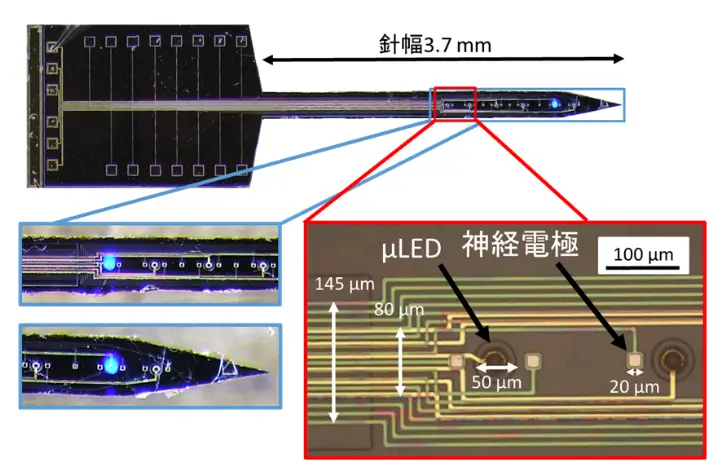
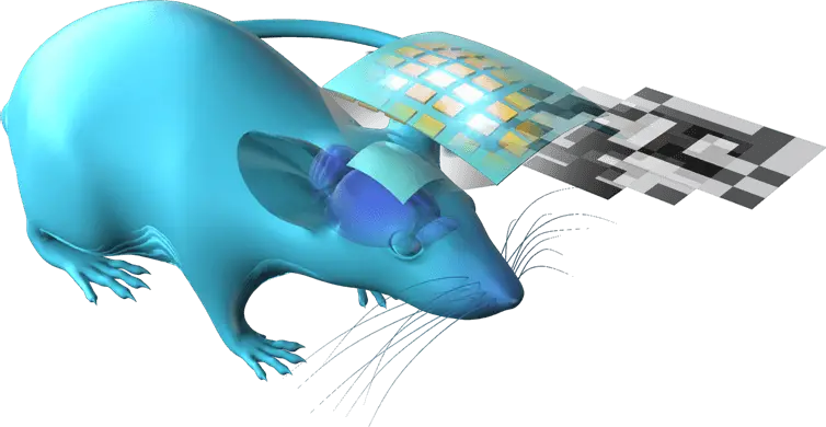
Our primary interest lies in fabricating microLEDs tailored for optogenetics, an innovative technology that enables precise manipulation of specific neurons through light and genetic modification, thereby regulating neural activity in living organisms. Our laboratory endeavors to develop an advanced light irradiation tool capable of controlling specific brain regions or multiple neural activities through developing microLEDs and implanting them into the living tissue. For example, we are actively designing needle-type microLED devices for tissue insertion and flexible microLED films for tissue coverage.
Please describe how your research journey began and how it has led you to your current position.
During my doctoral studies, I researched green and red LEDs using nitride semiconductor nanocolumn crystals under the guidance of Professor Katsumi Kishino, who is currently a guest professor at Sophia University. There was a demand for high-efficiency green and red LEDs using nitride semiconductors, but challenges arose due to crystal defects and internal electric fields at longer wavelengths. Our laboratory focused on nanocrystals, known as nanocolumns, which showed potential for fewer defects in crystals and suppression of internal electric fields. This led me to focus on fabricating light-emitting devices using these nanocrystals. One of my major achievements as a doctoral student was developing a technology to control the position and shape of nanocrystals, integrating RGB primary colors on the same substrate.�
While some time has passed since then, I am pleased that many researchers worldwide have referenced my papers. However, as an independent researcher, I feel the responsibility to establish valuable research themes. Although my research primarily focused on crystal growth, Professor Kishino encouraged me to consider the devices I wanted to fabricate and their practical applications. This guidance continues to influence my research approach, emphasizing the fabrication of usable devices with clear future goals.
After joining Toyohashi University of Technology in 2010, I conducted research under Professor Akihiro Wakahara (currently Director and Vice President of Toyohashi University of Technology) to develop a red LED by incorporating the rare earth element europium (Eu) into a nitride semiconductor. Additionally, gas lines and electrical equipment for Molecular Beam Epitaxy (MBE) were upgraded from those used for other material systems to facilitate crystal growth of GaN-based materials. Through the use of magnesium (Mg), we discovered that Eu in GaN emits strong luminescence, showing its potential for LED applications. Furthermore, we observed that incorporating Eu into nanocrystals revealed the potential to create devices with a higher luminescence intensity at elevated concentrations compared to thin film.
In my mid-thirties, I explored various avenues to broaden my research horizons. This included fabricating microLED arrays with a diameter of 30 µm by processing GaN-based LED wafers. Additionally, I contributed to the realization of monolithic integration with Si transistors through wafer bonding, exploring the fusion of polymer waveguides and LED arrays, and investigated integrated circuits using GaN-based transistors. Looking back, it was a time of searching for my own research theme and grappling with various challenges.
Since my student days, I have been fascinated by light, which is intangible but visible, and I have wanted to pioneer a new field of devices using visible light. During this time of seeking new possibilities as a researcher, I had a significant encounter that shaped my current research direction.
Around 2017, at my daughter’s kindergarten event, I discovered that a classmate’s father was a professor in the pharmacy department of another university. Our interaction was brief, but about six months later, I received an unexpected email from that professor asking if it would be possible to create LED devices for use in neuroscience research. Under normal circumstances, I might have declined such a request. However, I was actively exploring a different theme using visible light at that time, and I thought that we might leverage our university’s facilities for this purpose. This marked a significant turning point in my exploration of a new research field. Given the vast difference from my previous research, I believe I wouldn’t have pursued it if the timing had been slightly different, maybe a year or two earlier or later. It was a timely pursuit as I searched for a new research theme. This interaction became a significant catalyst for my exploration of new research fields.
My current research centers on developing an implantable biological tool to understand brain function mechanisms. Neural activity has historically been managed through medication or electrical stimulation. However, medication necessitates removing the previous dosage before administering the next. Additionally, electrical stimulation can inadvertently affect unintended areas. In contrast, light offers precise control over specific locations, enabling the study of the direct relationship between stimulation sites and neural activity. Optogenetic methods, prevalent in life science, provide this light-controlled neural activity regulation, thus creating a demand for devices capable of illuminating neurons at multiple points. We are actively working on developing microLED devices tailored for such applications.
Our research encompasses needle-like structures for deep tissue insertion, flexible microLED films for widespread neuron illumination, and evaluation techniques for ensuring device durability and effective temperature management during operation. Furthermore, I am actively involved in the development of electrocorticogram measurement devices, embedding them successfully in mice brains to acquire multisensory information simultaneously. The overarching goal is to integrate these devices into multifunctional tools capable of both manipulating and measuring neural activities accurately.

What are your future plans for your research?
Drawing on our expertise in microLED process technology, we aim to advance the development of bio-implantable devices capable of manipulating and measuring various neural activities. Although still in the developmental phase, these devices are gradually becoming applicable in cutting-edge neuroscience research. Our goal is to foster collaboration across different fields and to contribute to uncovering numerous undiscovered phenomena in life sciences by leveraging our electronics technology in the future.
Could you please share your thoughts on using our systems?

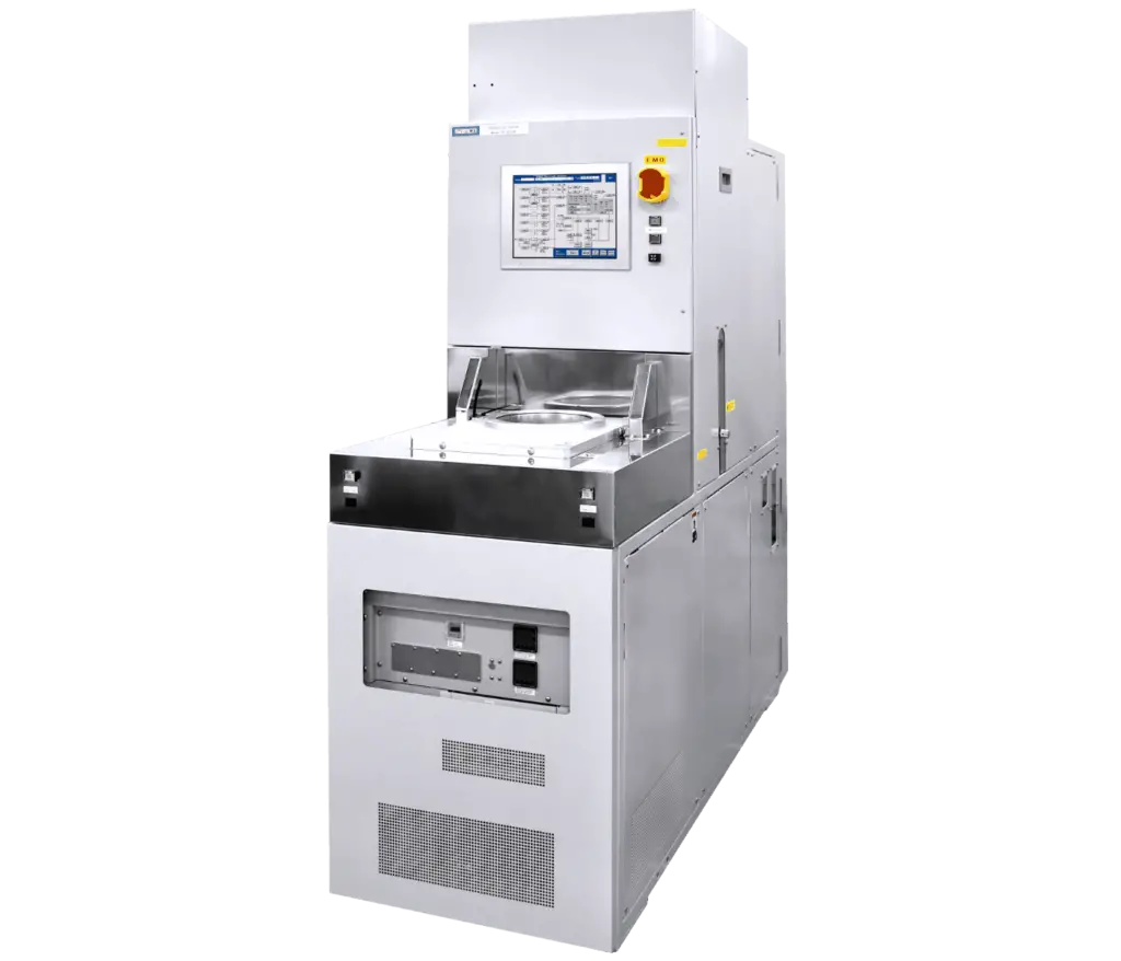
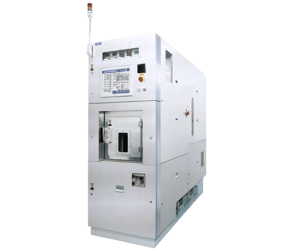
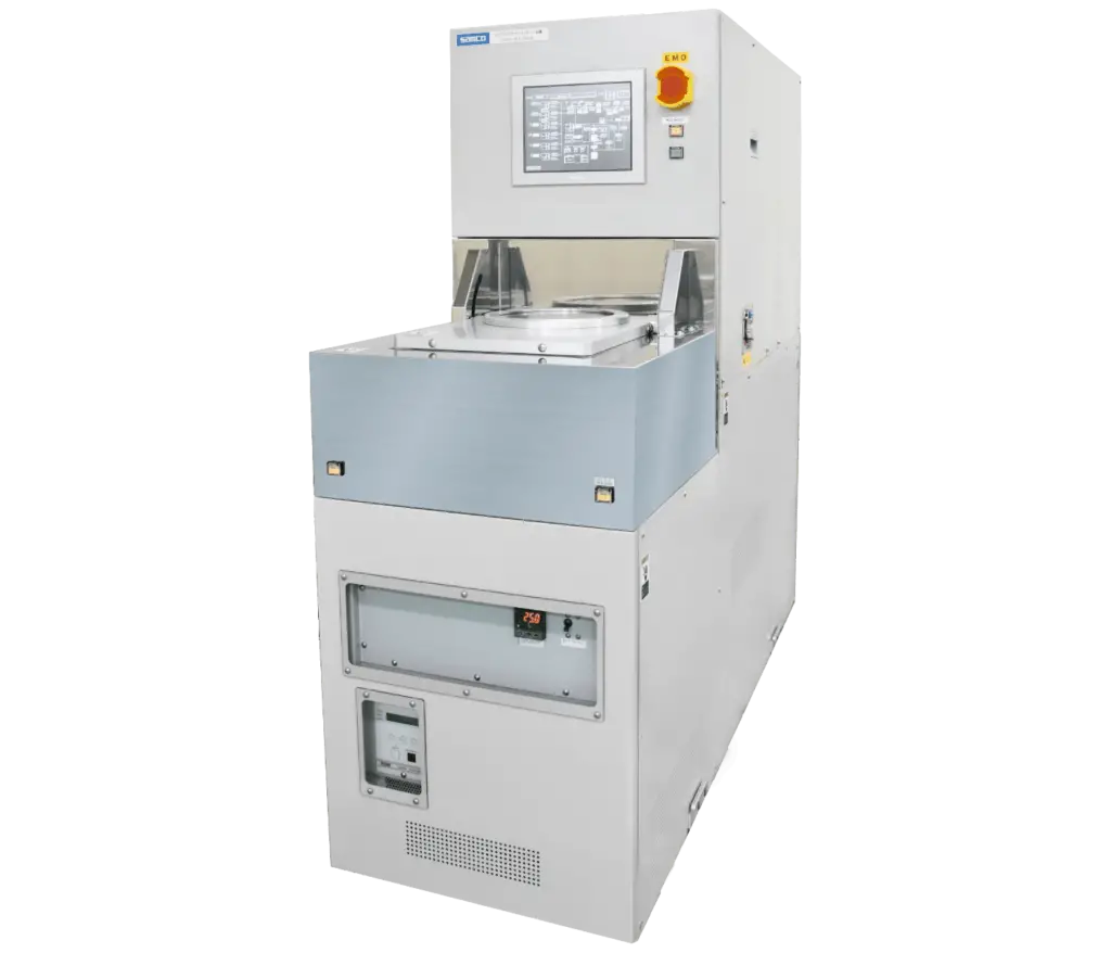
We have an ICP-RIE system (RIE-101iPH) for GaN or chlorine etching, two RIE systems (RIE-200NL, one each for chlorine and fluorine etching), and two plasma CVD systems (PD-220NL and PD-220N), some of which are shared. These systems are used for processing LED wafers, silicon, organic materials, and depositing SiO2 on wafers for insulation or protective films. All these systems share similar interfaces, making them user-friendly even for students. We find them highly convenient in our research because it is crucial to produce the same products repeatedly. Therefore, Samco’s systems are highly useful for device fabrication, enabling us to achieve high reproducibility while adjusting conditions.
In your daily research, what do you focus on?
I always strive to find interesting things, have fun working on them, and enjoy the time I spend doing it. I often recommend my students to take this approach as well. While discovering and understanding themes and challenges are crucial in research, I ask myself and my students if we are working on themes that bring joy with small achievements or just addressing immediate needs. Research often focuses on what’s immediately achievable, such as preparing for conferences. However, I believe it’s essential to aim for the ultimate goal and progress daily toward it.
How do you spend your holidays?
On my days off, I spend most of them relaxing at home or shopping with my family. I enjoy listening to podcasts and other audio programs. In my free time or while traveling, I listen to programs on Japanese and world history, economics and management, religion, and culture. I think it is important to acquire a wide range of knowledge and perspectives. Furthermore, going out is more about experiencing something new than just shopping. Exploring different environments and walking in unfamiliar places help me to relax and refresh both mentally and physically, often leading to new research ideas.
Any final words?
As semiconductor technology continues to gain increasing attention, I believe there will be a growing demand worldwide for research and development across various fields in semiconductor technology. I have the impression that Samco develops user-friendly systems for university researchers and offers a lineup of various types of equipment. Universities will continue to develop materials and devices in small quantities but with a wide variety, so I hope that Samco will continue to meet detailed requirements and provide highly reproducible and relatively affordable systems.
Thank you very much for taking time out of your busy schedule to speak with us.